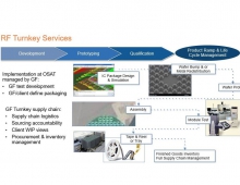
GLOBALFOUNDRIES Calls for Renewed Focus on 300mm Manufacturing Innovation
At SEMICON West, the GLOBALFOUNDRIES describes the need for increasing efficiency and minimizing waste in the 300mm manufacturing process.
In its effort to meet the ever-increasing demands of consumer technology, the semiconductor industry has long been preoccupied with smaller transistors and larger silicon wafers. While these are important tactics, opportunities for increasing efficiency, becoming more agile, and minimizing waste are often overlooked in manufacturing processes, according to Thomas Sonderman, vice president of manufacturing systems and technology at GLOBALFOUNDRIES.
At SEMICON West 2009, Sonderman is calling for a renewed focus on operational agility in the semiconductor manufacturing industry, particularly in light of increased pressure to move to processes based on 450 millimeter (mm) wafers.
"The rush to 450mm suggests a lack of ideas for improving fab productivity," Sonderman said. "At GLOBALFOUNDRIES, we see a tremendous amount of headroom left in the 300mm process. We are tapping our expertise in lean manufacturing to extend the lifecycle of the industrys current 300mm investments, and we are investing more than $4 billion in a new, state-of-the-art 300mm fab in upstate New York because we are confident in our ability to get the most out of this technology generation."
Sonderman will be participating today in the SEMICON West Foundry Summit, a two-hour panel discussion on the market strategies, technologies, capital spending, and other strategic plans of the world's major chip foundries. He cites GLOBALFOUNDRIES rapid transition and time to mature yield at the 45 nanometer (nm) process node as a model for operational efficiency in the industry.
During the transition to 45nm, GLOBALFOUNDRIES claims that it has achieved the fastest time to mature yield of any process in its history, while simultaneously implementing a complex new form of lithographyimmersion lithographyahead of all other semiconductor manufacturers.
Immersion lithography allows for enhanced microprocessor design definition and manufacturing consistency by placing a fluid, instead of air, between the final element of the lens of a lithographic exposure tool and the wafer.
All wafer starts in Fab 1, Module 1 have now been converted to 45nma process that is proving to deliver few defects, low leakage, and high performance. GLOBALFOUNDRIES and AMD recently announced the launch of a six-core processor codenamed "Istanbul," which was manufactured using the 45 nm process. "Istanbul" is the most complex processor ever designed by AMD, and GLOBALFOUNDRIES manufacturing agility allowed AMD to deliver "Istanbul" five months ahead of schedule.
"The agility and execution of our design and engineering teams combined with the leading-edge manufacturing of GLOBALFOUNDRIES made possible an early, well-executed delivery of Six-Core AMD Opteron processors to customers," said Rick Bergman, senior vice president and general manager of the AMD Products Group. "As our silicon designs get ever more complex, it is critical to retain this close collaboration and reliable execution as we deliver the next wave of processing innovation on the x86 platform."
A key to GLOBALFOUNDRIES operational agility is a model based on highly automated decision-making and "lean" manufacturing principles, called Automated Precision Manufacturing (APM). APM allows GLOBALFOUNDRIES to precisely tune manufacturing operations to align production with customer demandall while minimizing waste and reducing cycle time, inventory, and ultimately costs.
APM will be taken to the next level with the construction of Fab 2an estimated $4.2 billion project to build the worlds most advanced 300mm semiconductor foundry in Saratoga County, N.Y.
"When Fab 2 begins volume production in approximately 2012, it will be part of an integrated global network linked by the next generation of APM," said Norm Armour, vice president and general manager of GLOBALFOUNDRIES Fab 2. "The next generation of APM will feature interoperable technologies across multiple fabs and the implementation of lean processes in all aspects of manufacturing, from the front end of the supply chain to the final wafers out the door of the fab."
Armour will participate today in the annual SEMI Press Luncheon at SEMICON West, where he will present a history of the Fab 2 project and an overview of the capabilities of the new leading-edge facility, which is being designed to support 28/22nm process technologies.
GLOBALFOUNDRIES is a semiconductor manufacturing company. The company was launched in March 2009 through a partnership between AMD and the Advanced Technology Investment Company (ATIC).