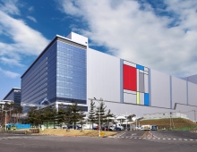
TSMC Tapes out First 5nm Chip, Outlines Packaging Techniques
TSMC has taped out its first chip in a process that partially makes use of extreme ultraviolet lithography (EUV) and will start risk production in April on a 5nm node with full EUV. The foundry also gave an update on the packaging techniques it is developing to speed connections between chips.
TSMC announced it taped out a customer chip in a N7+ node that can use EUV on up to four layers. Its N5 that will use EUV on up to 14 layers will be ready for risk production April. EUV aims to lower costs by reducing the number of masks required for leading-edge designs.
The N7+ node sports a tighter metal pitch and includes a single-fin library that can help lower dynamic power. It will be available in a version for automotive designs by April. N7+ offers "nearly the same analog performance as N7," said Cliff Hou, vice president of technology development at TSMC.
Transistor density at N7 is 16.8x greater than at the foundry's 40nm node, TSMC said.
TSMC said N5 will deliver 14.7 to 17.7% speed gains and 1.8-1.86 area shrinks based on tests with Arm A72 cores. The N7+ node can deliver 6-12% less power and 20% better density.
Chip designs for the N5 node can start today, although most EDA tools won't hit a 0.9-version readiness until November. Many of TSMC's foundation IP blocks are ready for N5, but some including PCIe Gen 4, USB 3.1 may not be ready until June.
Meanwhile, rival Samsung is ramping a 7nm node using EUV. Intel is not expected to use EUV anytime soon, while Globalfoundries announced in August it has halted work on 7nm and EUV.
TSMC also outlined the two flavors of a planar 22nm processes. It aims to compete with fully depleted silicon-on-insular processes from Globalfoundries and Samsung. GF announced late last month it has more than 50 design wins for its 22nm version of FD-SOI.
Engineers can start designs before the end of the year on TSMC's 22ULP and ULL processes that generally use 28nm design rules and support 0.8-0.9V. Some IP will not be available for the 22nm nodes until June, including PCIe Gen 4, DDR4, LPDDR4, HDMI 2.1 and USB 3.1 blocks.
The ULP version offers up to 10% speed gains or 20% less power and a 10% shrink over its 28 HPC+. The ULL version aims at lowest power for designs such as Bluetooth chips. By April a version will be ready supporting voltages from 1.05-0.54V with more optimization for analog circuits.
In packaging, TSMC uses four wafer-level fan-out options.
InFO-on-Substrate is a chip-first process using two-micron interconnects between SoCs and 40nm SoC I/O pitches. It has been qualified on 65mm2 chips now in production. The foundry aims to expand it to components at 1.5x reticle size.
InFO-Memory-on-Substrate will be qualified for production by the end of the year. It can link logic and typically HBM memory on a full reticle 830mm2 device.
The 2.5D process TSMC calls CoWoS will shrink from using a 180-150-micron C4 bump pitches now to 130-micron pitches by the end of the year. It will expand from 1.5x reticle to 2x reticle by April to support a class of designs such as large GPUs and some networking ASICs.
System on Integrated Chips (SoIC) will have EDA support and foundry qualification for starting designs before May. The approach puts one or two chips on top of another using through silicon vias connecting bumps with a pitch of less than 10 microns.
Bring chip design to the cloud
Separately, TSMC announced it has worked with Amazon Web Services, Cadence, Microsoft Azure and Synopsys to enable back-end chip design based in the cloud. The so-called Virtual Design Environment initially will use "store fronts" created by Cadence and Synopsys to support digital RTL-to-GDSII and custom schematic-capture-to-GDSII flows.
TSMC expects other EDA vendors will eventually join the effort that also will come to include front-end design flows. To test out the capabilities, TSMC is designing its N5 SRAM using the service. In addition, Synopsys used it to tape out a PCIe Gen 5 PHY block in TSMC's 7nm node, and startup SiFive used it to design a 28nm RISC-V core.
Initially, customers need to engage one of the partners to create a custom site for them based on user requirements and license agreements. Partners declined to comment on liability for any IP theft, likely an element of those business agreements.