Research Breakthrough Paves Way for Post-Silicon Future
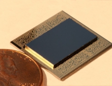
IBM Research today announced an engineering breakthrough that could accelerate carbon nanotubes replacing silicon transistors to power future computing technologies. IBM scientists demonstrated a new way to shrink transistor contacts without reducing performance of carbon nanotube devices, opening a pathway to faster, smaller and more powerful computer chips beyond the capabilities of traditional semiconductors.
IBM's breakthrough overcomes a major hurdle that silicon and any semiconductor transistor technologies face when scaling down. In any transistor, two things scale: the channel and its two contacts. As devices become smaller, increased contact resistance for carbon nanotubes has hindered performance gains until now. These results could overcome contact resistance challenges all the way to the 1.8 nanometer node – four technology generations away.
Carbon nanotube chips could greatly improve the capabilities of high performance computers, enabling Big Data to be analyzed faster, increasing the power and battery life of mobile devices and the Internet of Things, and allowing cloud data centers to deliver services more efficiently and economically.
Silicon transistors have been made smaller year after year, but they are approaching a point of physical limitation. With Moore's Law running out of steam, shrinking the size of the transistor – including the channels and contacts – without compromising performance has been a vexing challenge troubling researchers for decades.
IBM has previously shown that carbon nanotube transistors can operate as excellent switches at channel dimensions of less than ten nanometers – the equivalent to 10,000 times thinner than a strand of human hair and less than half the size of today’s leading silicon technology. IBM's new contact approach overcomes the other major hurdle in incorporating carbon nanotubes into semiconductor devices, which could result in smaller chips with greater performance and lower power consumption.
Earlier this summer, IBM unveiled the first 7 nanometer node silicon test chip, pushing the limits of silicon technologies and ensuring further innovations for IBM Systems and the IT industry. By advancing research of carbon nanotubes to replace traditional silicon devices, IBM is paving the way for a post-silicon future and delivering on its $3 billion chip R&D investment announced in July 2014.
Carbon nanotubes represent a new class of semiconductor materials that consist of single atomic sheets of carbon rolled up into a tube. The carbon nanotubes form the core of a transistor device whose superior electrical properties promise several generations of technology scaling beyond the physical limits of silicon.
Electrons in carbon transistors can move more easily than in silicon-based devices, and the ultra-thin body of carbon nanotubes provide additional advantages at the atomic scale. Inside a chip, contacts are the valves that control the flow of electrons from metal into the channels of a semiconductor. As transistors shrink in size, electrical resistance increases within the contacts, which impedes performance. Until now, decreasing the size of the contacts on a device caused a commensurate drop in performance – a challenge facing both silicon and carbon nanotube transistor technologies.
IBM researchers had to forego traditional contact schemes and invented a metallurgical process akin to microscopic welding that chemically binds the metal atoms to the carbon atoms at the ends of nanotubes. This 'end-bonded contact scheme' allows the contacts to be shrunken down to below 10 nanometers without deteriorating performance of the carbon nanotube devices.