TSMC Talks About 7nm, 6nm and 5nm Processes, Packaging
TSMC has added an N5P process and takled about its advanced packages at its North American Technology Symposium in San Fransisco held on April 23.
The event highlighted TSMC’s breakthroughs in advanced logic technology, specialty technology, advanced packaging and more.
TSMC’s N5 process started risk production in March and will offer 80% more density and 15% more speed or 30% less power than its N7 node now in volume production, according to the company. Using new eLVT transistors, speed gains could hit 25%.
The N5P starting risk production next year could squeeze another 7% in speed or 15% in power from N5 using the same design rules. The gains come in part from enhancements to a fully strained high-mobility channel.
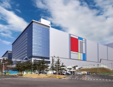
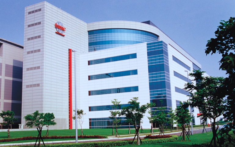
TSMC showed an N5 wafer with SRAM yields above 90% and logic yields above 80% from the first phase of its new Fab 18. Shells for two more phases are under construction. A few key IP blocks for N5 such as PAM4 SerDes and HBM blocks are still in development.
N6 lacks the performance and power boosts of N5 but will offer an 18% shrink over N7 (8% over N7+) and uses existing N7 design rules and blocks. However, N6 won’t start risk production until Q1 2020, and a key design library for M0 routing is still in development.
Last week, Samsung announced that it had taped out a chip in what it described as a custom 6-nm process.
TSMC is using extreme ultraviolet lithography on “a few critical layers” for N7+, the foundry’s first EUV process starting volume production in Q3 2019. N6 uses one additional EUV layer and N5 adds “more layers.” Designers should see about a 10% mask decrease due to EUV at N7+ and additional reductions at N6 and N5.
The latest EUV machines support a stable 280-W light source that TSMC expects to hit 300 W by the end of the year and greater than 350 W in 2020. Uptime increased from 70% last year to about 85% today and should hit 90% next year.
TSMC reported on research paving a path to 3-nm and 2-nm nodes but stopped short of describing new transistors they will require. Sulfide and selenide 2D materials promise good mobility as channel thickness drops below 1 nm and can deliver higher drive current than silicon at 7-nm gate lengths, according to Yuh-Jier Mii, a senior vice president for technology development for TSMC.
The foundry developed a new low-k film more resistant to depletion effects as chip dimensions shrink. It also showed regular metal lines made at 30 nm using a new reactive ion etch process.
TSMC also said that its 22ULL node will support 0.6–0.9 voltages for battery-operated chips. HDMI blocks are still being developed and USB, MIPI, and LPDDR blocks are still being qualified for the process that is an upgrade of its 28-nm node.
In packaging, TSMC provided new details on its latest options — SoIC and Wafer-on-Wafer. WoW only works with two die of the same size, while SoIC can stack multiple die of different sizes. Both target mobile and high-performance computing systems but are still in development with commercial products not expected until 2021.
Both options are front-end processes that bond die directly using copper pads with interconnect pitches starting at 9 microns. Through-silicon vias (TSVs) make connections to external micro-bumps.
By Q3, TSMC will provide macros as a starting point for TSV designs. Thermal models will follow by the end of the year.
Meanwhile, the foundry is extending its 2.5D CoWoS process this year to support devices twice the reticle size. Next year, it will expand to 3× the reticle size and support for five metal layers with deep trench capacitors in the silicon substrate to ease signal and power integrity challenges.
TSMC also reported advances across about seven different specialty processes that it offers for embedded memory, image sensors, MEMS, and other components. Increasingly, it aims to package them as modules closely tied to logic nodes.
In RF-SOI, it is moving 180-nm capabilities on 200-mm wafers to a 40-nm node on 300-mm wafers. For 5G phones, it is optimizing 28-/22-nm nodes for millimeter-wave (mmWave) front-end modules and its 16FFC node for mmWave and sub-6-GHz transceivers.
For microcontrollers, embedded MRAM started risk production in a 22-nm node last year and resistive RAM will start risk production in the node later this year.