Samsung Electronics Announced MBCFET Transistor Structure For Advanced Foundry Nodes
Samsung has created and patented the proprietary MBCFET (Multi-Bridge Channel Field Effect Transistor), an optimized version of the GAA transistor, laying out the foundation for transforming the semiconductor industry that was set to stall at the 4-nanometer scale.
MBCFET was announced at the Samsung Foundry Forum 2019 USA event, held today in Santa Clara, California.The company also provided an update on its process technology and packaginf roadmaps.
In order to understand the improtance of MBCFET, let's takl about the basics of transistors and its evolution in time.
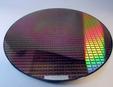
A transistor is a semiconductor device used to transform the digital information coded in the binary system into electric signals. A transistor is composed of a ‘channel’ in which the electric current flows between the semiconductor’s source and its drain and a ‘gate’ for managing the electric current traveling through the channel. The gate generates binary system data by amplifying electric signals and also working as a switch. Because of this, the transistor is essentially the basic element of a semiconductor chip.
In order to increase the number of semiconductor chips mounted on the limited surface of a silicon (Si) substrate, the size of each semiconductor chip naturally needs to be decreased. Furthermore, in order to fit more new and complex functions into each semiconductor chip, the very basic element transistor must become smaller and its power consumption must be minimized to provide the longest possible battery lifespan, as well as reduced heat and electric charges. As electricity consumption is dependent on operating voltage, transistors have been developed so as to decrease operating voltage. Therefore, the history of the semiconductor is synonymous with the history of creating transistors that are smaller, faster and that consume less electricity.
The most widely used transistor in the current semiconductor industry is the Metal-Oxide-Semiconductor (MOS). It consists of a metal electrode, an oxide insulator and a semiconductor channel. The first MOS transistor was of a planar architecture and was structured so that the gate and the channel made contact on one plane. But, as transistors become smaller, the distance between the source and the drain gets smaller, making it difficult for the transistor to work as a switch. This is called a ‘short-channel effect’, and along with limiting voltage reduction, it means that planar transistors can only be applied to 20 or above nanometer nodes (or generations).
In order to overcome the short-channel effect, the Fully Depleted transistor emerged as the next generation of transistor. This transistor uses a thin silicon (Si) channel to avoid the short-channel effect by enhancing the ability of the gate to adjust the channel. Its structure format evolved out of that of the conventional transistor (a gate on a plane channel) to become a thin, rugged structure with a standing rectangular channel that interlocks with gates on three sides. As this thin, standing channel somewhat resembles a fish’s dorsal fin, it is also called the ‘fin transistor’. Samsung manufactures fin transistors in a range of sizes, starting at just 14 nanometers.
Whereas a planar transistor only allows the channel and the gate to contact in just one plane, a fin transistor has a 3-dimensional structure that allows three sides of a channel (excluding its bottom) to come into contact with the gates. This increased contact with the gates improves semiconductor performance as well as increasing the reduction of operating voltage, solving the problems brought about by the short-channel effect.
Nevertheless, the fin transistor is now facing limitations after several generations of developments and process transitions. Nowadays, the semiconductor industry is increasingly requiring transistors that can reduce operating voltage even further. Despite the fin transistor’s 3-dimensional structure, that only three of the four sides are in contact with gates is now becoming a limitation, as transistors themselves continue to progress and subsequently get smaller.
![]()
![]()
In order to mitigate the limitations of existing transistors solutions, Samsung has developed a new structure, the Gate-All-Around (GAA). As the name suggests, the GAA is a structure that maximizes gates’ channel-controlling function, as all channels, including the fourth bottom one, are covered by gates. The gates provide a 360-degree coverage of the entire channel area to eliminate the short-channel effect, resulting in reducing operating voltage further.
A typical GAA transistor takes the form of a thin and long nanowire. However, a channel needs to be as wide as possible in order to allow a large amount of current to flow through it, and the small diameter of the nanowire makes obtaining this higher current flow difficult. To overcome this, Samsung created and patented their proprietary MBCFET (Multi-Bridge Channel Field Effect Transistor), an optimized version of the GAA transistor. The MBCFET increases the areas that make contact with gates by aligning wire-formed channel structures as a 2-dimensional nanosheets, which enables simpler device integration as well as increasing the electric current. Samsung says that the MBCFET is a competitive transistor structure in that it not only includes the means to mitigate the short-channel effect thanks to the GAA structure, but it also increases performance by expanding the channel area.
![]()
![]()
In addition, MBCFETs compatibility with FinFET processes means the two can share the same manufacturing technology and equipment, which accelerates process development and production ramp-up.
Compared to existing 7-nanometer fin transistor process technology, the MBCFET or 3nm Gate-All-Around (GAA) process, 3GAE, decreases power consumption by 50%, improves performance by 30%, and reduces the area that the transistor takes up by 45%, Samsung claims.
Voltage scaling of FinFET technology runs out of steam at 0.75V at the 10nm node. Samsung's GAA technology reduces the operating voltage to 0.7V.
The development of GAA transistors is such a difficult process that Samsung is currently offering a future delivery plan. The company said that its 3nm GAA (3GAE) development is on track. The company noted today that its Process Design Kit (PDK) version 0.1 for 3GAE has been released in April to help its customers get an early start on the design work and enable improved design competitiveness along with reduced turnaround time (TAT).
The GAA-based process node is expected to be widely adopted in next-generation applications, such as mobile, network, automotive, Artificial Intelligence (AI) and IoT.
Samsung recently taped out the 3GAE test vehicle design and will focus on improving its performance and power efficiency going forward. The company plans to begin risk production of one of two 3-nm GAA processes it plans to offer by the second half of next year, with mass production expected in 2021. The company plans to begin risk production of the next 3nm GAA process in 2021, with mass production expected in 2022.
“We stand at the verge of the Fourth Industrial Revolution, a new era of high-performance computing and connectivity that will advance the daily lives of everyone on the planet,” said Dr. ES Jung, President and head of Foundry Business at Samsung Electronics.
“Samsung Electronics fully understands that achieving powerful and reliable silicon solutions requires not only the most advanced manufacturing and packaging processes as well as design solutions, but also collaborative foundry-customer relationships grounded on trust and shared vision. This year’s Foundry Forum is filled with compelling evidence of our commitment to progress in all those areas, and we’re honored to host and converse with our industry’s best and brightest,” Dr. Jung added.
New SAFE–Cloud Program
As part of its efforts to support and enhance customers’ entire design workflow, Samsung also launched the Samsung Advanced Foundry Ecosystem Cloud (SAFE-Cloud) program. It will provide the company's customers with a more flexible design environment through collaboration with major public cloud service providers, such as Amazon Web Services (AWS) and Microsoft Azure, as well as leading Electronic Design Automation (EDA) companies, including Cadence and Synopsys.
To date, most foundry customers have built and managed design infrastructure on their own servers. The SAFE-Cloud program reduces this burden and supports easier, faster and more efficient design efforts by providing a turnkey design environment with extensive process information (PDK, design methodologies), EDA tools, design assets (IP, library) and design services.
Utilizing the SAFE-Cloud platform, Samsung was able to accelerate the development of its 7nm and 5nm cell libraries in collaboration with Synopsys. In addition, Samsung, Gaonchips – a fabless design company in Korea – and Cadence have successfully completed design verification based on the platform.
Process Technology Roadmap and Advanced Packaging Updates
Samsung’s roadmap includes four FinFET-based processes from 7nm down to 4nm that leverage extreme ultraviolet (EUV) technology as well as 3nm GAA, or MBCFET. Last month, Samsung began volume production on its 7-nm FinFET process, the first to make use of EUV lithography. While the company plans to roll out derivative 6-, 5- and 4-nm processes with FinFETs over the next two to three years, Samsung considers 3-nm to be its next major process technology node.
In the second half of this year, Samsung is scheduled to start the mass production of 6nm process devices and complete the development of 4nm process.
The product design of Samsung’s 5nm FinFET process, which was developed in April, is expected to be completed in the second half of this year and go under mass production in the first half of 2020.
Rival TSMC is planning to introduce its version of GAA technology at the 5-nm node, but has not announced a target date for putting the technology in production.
Samsung is considerd to have a one-year lead in GAA over TSMC, thanks to its heavy investment in R&D on advanced materials, including graphene.
Still, generation-to-generation process technology improvements in process technology continue to decline. Compared to its 7-nm technology, Samsung 5-nm process improves logic density by just 25%, he said. The 3-nm GAA process adds just 20% improvement on top of that.
Extensions of the company’s FD-SOI (FDS) process and eMRAM together with an expanded set of package solutions were also unveiled at this year’s Foundry Forum. Development of the successor to the 28FDS process, 18FDS, and eMRAM with 1Gb capacity will be finished this year.