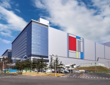
Questions Remain on TSMC's 7nm, 5nm Gains
TSMC has announced it is in volume production with a 7nm process and will have a version using extreme ultraviolet (EUV) lithography ramping early next year, but the advantages with the new process nodes are getting thinner.
The Taiwanese giant also provided its first timeline for a 5nm node and announced a half dozen new packaging options.
According to TSMC, the performance gains and power reductions that will be seen from moving forward the CMOS scaling falls in just the 10-20 percent range.
Currently, TSMC's new 7nm chips deliver 35 percent more speed or uses 65 percent less power and sports a 3x gain in routed gate density. By contrast the N7+ node with EUV will only deliver 20 percent more density, 10 percent less power and apparently no speed gains. In addition, these advances require use of new standard cells.
TSMC has validated in silicon what it calls foundation IP for N7+. However, several key blocks will not be ready until late this year or early next year, including 28-112G serdes, embedded FPGAs, HBM2 and DDR5 interfaces.
Cliff Hou, vice president of R&D for design and technology platforms at TSMC, said that fully certified EDA flows for N7+ will be ready by August. Meanwhile, yields of a test 256-Mbit SRAM at N7+ are as good as yields were for the early 7nm node, he said.
Looking ahead, TSMC aims to start risk production of a 5nm node late next year, focusing on mobile and high-performance computing chips.
Compared to the initial 7nm without EUV, the 5nm node promises a 1.8x greater density than 7nm. However, it is only expected to reduce power by up to 20 percent or raise speeds by about 15 percent, perhaps 25 percent using a new device option.
ASML.
It appears that TSMC's EUV plan is within six months of the production schedule of Samsung, which has said it will be in production this year.
By the end of 2019, the TSMC aims to triple to 1.1 million wafers/year its production on 10/7nm nodes.
In terms of packaging, TSMC has established its 2.5-D CoWoS package in GPUs and other processors and its wafer-level fan-out InFO in smartphone chips.
CoWoS chips will have options for silicon interposers up to twice a reticle's size, starting early next year. Versions with 130-micron bump pitch will be qualified this year.
Variants of the InFO technique are Info-MS, InFO-oS and InFO-AIP.
Info-MS will be used for memory substrate. It packs an SoC and HBM on a 1x reticle substrate with a 2x2-micron redistribution layer and will be qualified in September.
InFO-oS has a backside RDL pitch better matched to DRAM and is ready now. A multi-stacking option puts one or two chips on top of another larger one linked through an interposer at the base of the stack.
InFO-AIP stands for antenna-in-package, sporting a 10 percent smaller form factor and 40 percent higher gain. It targets designs such as front-end modules for 5G basebands.
TSMC has also introduced two new packaging options.
A wafer-on-wafer pack (WoW) directly bonds up to three dice. It was released last week, but users need to ensure their EDA flows support the bonding technique. It will get EMI support in June.
Finally, the foundry talked about system-on-integrated-chips (SoIC) using less than 10-micron interconnects to link two dice.
But improvements are not only coming to the nodes lower than 8nm.
The company is developing ultra-low power and ultra-low leakage versions of its 22nm planar and 12nm FinFET nodes. They will compete with FD-SOI processes ramping at Globalfoundries and Samsung.
The new 22nm versions use 28nm design rules and deliver a 10 percent optical shrink and speed gain or can reduce power 20 percent. The process and related IP will be ready by the end of the year with target apps including advanced microcontrollers, IoT and 5G millimeter wave chips.
The 12nm versions use FinFETs and more compact cell libraries to deliver about 16 percent more speed than TSMC's 16FFC. High-speed serdes are among the few pieces of IP that won't be ready until next year.
In memories, a 40nm resistive RAM is now ready as an alternative to flash for IoT chips. It adds just two mask layers and sports 10 years of retention and support for 10,000 cycles.
Moving forward, TSMC researchers are progressing on designs of stacked nanowires as nanosheets for a next-generation transistor suitable for work at 2nm and beyond. The design sports better electrostatics than FinFETs and can be optimized for power and performance by adjusting device width.
The foundry sees germanium as a strong candidate to replace silicon, providing lower power at the same speed. It achieved a record low contact resistance using the material in a CMOS-compatible dielectric.
In memories, they are exploring embedded MRAM for use beyond the 22nm node, possibly with alternative magnetic structures.