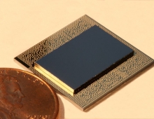
IBM Uses Graphene to Place Nanomaterials on Wafers, Moore's Law Rescued?
IBM researchers are using graphene to deposit nanomaterials in predefined locations without chemical contamination, pushing beyond 7 nanometers chip making process.
In research described in the journal Nature Communications, the IBM researchers for the first time electrified graphene so that it helps to deposit nanomaterials with 97% accuracy.
Nanomaterials offer unique optical and electrical properties and bottom-up integration within industrial semiconductor manufacturing processes. However, they also present one of the most challenging research problems. In essence, semiconductor manufacturing today lacks methods for depositing nanomaterials at predefined chip locations without chemical contamination. IBM researchers believe that graphene, one of the thinnest, strongest, most flexible and most conductive materials on the planet, could help solve this manufacturing challenge.
The team, the Industrial Technology and Science group in IBM Research-Brazil, is focused on the building, application, and adoption of nanomaterials (which are one millionth of a millimeter in size) for large-scale industrial applications. Until about 30 years ago, it wasn't possible to see and manipulate single atoms and molecules. With the development of new techniques, the researchers can start to experiment and theorize about the impact of a material's behavior at the nanoscale.
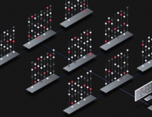
In new paper, "Graphene-enabled and directed nanomaterial placement from solution for large-scale device integration", published in Nature Communications, the researchers proved for the first time that is possible to electrify graphene so that it deposits material at any desired location at a solid surface with an almost-perfect turnout of 97%. Using graphene in this way enables the integration of nanomaterials at wafer scale and with nanometer precision.
Not only is it possible to deposit material at a specific, nanoscale location, the researchers also reported that this can be done in parallel, at multiple deposition sites, meaning it's possible to integrate nanomaterials at mass scale.

Graphene is the thinnest material capable of conducting electricity and propagating electric fields. The electric fields are what the researchers use to place nanomaterials on a graphene sheet: the shape and pattern of the graphene determines where the nanomaterials are placed. This offers an unprecedented level of precision for building nanomaterials. Today, this approach is done using standard materials, mostly metals such as copper. But the challenge occurs because it is nearly impossible to remove the copper from the nanomaterials once it's been assembled, without impacting the performance or destroying the nanomaterial completely. Graphene not only gives us precision in placement of nanomaterials, but is easily removable from the assembled nanomaterial.
Importantly, the method works regardless of the nanomaterial's shape, for example, with quantum dots, nanotubes, and two-dimensional nanosheets. The researchers have used the method to build functioning transistors and to test their performance. In addition to integrated electronics, the method may be utilized for particle manipulation and trapping in lab-on-chip (microfluidics) technology.
The advancement in using graphene for nanomaterial placement could be used to create next-generation solar panels, faster chips in cell phones and tablets, or exploratory quantum devices, like an electrically controlled, on-chip quantum light emitter or detector.
But this process is not going to come to the rescue of Moore's Law overnight. One of the biggest challenges is introducing solution-based nanomaterials into the industrial-scale manufacturing process.
The researchers are continuing to work on the device level of the technology with the integration of different nanomaterials in order to customize basic integrated circuits such as, for example, electrical inverters or ring oscillators.