Breaking News

be quiet! announces new Power Zone 2 1200W and Pure Power 13 M 1200W Thypoch announces 21mm f/3.5 M Mount Lens ASUS showcases new AI technologies and celebrates 20 years of ROG gaming at CES Prograde Digital Announces Pro Card Caddy COLORFUL GeForce Graphics Cards Harness NVIDIA DLSS 4.5 Cutting-Edge Gaming Technology

logo

  • Share Us
    • Facebook
    • Twitter
  • Home
  • Home
  • News
  • Reviews
  • Essays
  • Forum
  • Legacy
  • About
    • Submit News

    • Contact Us
    • Privacy

    • Promotion
    • Advertise

    • RSS Feed
    • Site Map

Search form

TSMC And IBM Detail Their 7nm Progress At 2016 IEDM

TSMC And IBM Detail Their 7nm Progress At 2016 IEDM

Enterprise & IT Dec 6,2016 0

TSMC and IBM has presented separate papers at the International Electron Devices Meeting (IEDM), describing their respective results nudging forward both Moore's law and extreme ultraviolet lithography (EUV).

IBM has been supporting the use of EUV while TSMC has been more conservative.

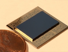
TSMC announced the smallest 6T SRAM to date in a process that it aims to put into risk production by April.

TSMC's 256-Mbit SRAM test chip has a cell density of 0.027 mm2 with full read/write capabilities down to 0.5 V. The node should provide up to a 40% speed gain, a 65% power reduction, and a 3.3x routed gate density increase compared to TSMC's 16FF+ process now in volume production.

Commenting on work using the 7-nm process to validate EUV TSMC's executives said that the next generation lithography provided "comparable patterning fidelity" and "comparable yield" to the conventional immersion steppers it will use in the commercial 7-nm process next year. TSMC already announced its plans to start using ASML's EUV equipment in its 5-nm node.

However, TSMC did not comment on how the 7-nm process compares to its 10-nm node or nodes from rivals such as Samsung. But the company said that it had reached 50% yields on its 7nm SRAM. That suggests it is on a path to have volume manufacturing in the process by late 2017.

IBM described the smallest FinFET made to date in a research device made with EUV. The company showed FinFETs with contacted poly pitch of 44/48 nm, a metallization pitch of 36 nm, and a fin pitch of 27 nm. One device included a source-to-drain contact opening of about 10 nm and a gate length of about 15 nm.

The IBM paper described EUV use at multiple critical levels in the middle and back-end of line, including M1 lines and novel metal interconnects, "greatly enhancing the printability and process simplification."

The 27-nm fin was made with a self-aligned quad patterning process using a 2x sidewall-image-transfer technique. IBM used self-aligned double patterning for making gates.

The transistors used cobalt rather than tungsten to reduce both line and vertical resistance.

The pitches on IBM?s research chip leapfrog the 56-nm gate pitch that Intel announced in August for its 10-nm process, claiming industry-leading density for the node it aims to have in production next year.

When Samsung announced its 10-nm process recently, it said that it would skip a version of 7 nm using today's immersion lithography. Instead, it said it will roll out 7 nm with EUV, targeting production before the end of 2018.

Globalfoundries has said that it developed its own 7-nm process using immersion steppers that will be in production in 2018.

Tags: EUV LithographyTSMCIBM
Previous Post
U.S. Supreme Court Rules in Favor of Samsung in Smartphone Patent Suit
Next Post
Oculus Touch Now Available

Related Posts

  • IBM and AMD Join Forces to Build the Future of Computing

  • IBM Unveils watsonx Generative AI Capabilities to Accelerate Mainframe Application Modernization

  • TSMC to boost 5nm chip output in 2H21

  • New magnetic tape prototype breaks data density and capacity records

  • IBM Expands the Computational Power of its IBM Cloud-Accessible Quantum Computers

  • TSMC Announces 7nm Automotive Design Enablement Platform

  • Samsung Expands its Foundry Capacity with A New 5nm Chip Production Line in Pyeongtaek, Korea

  • Synopsys and TSMC Collaborate to Enable Designs of HPC, Mobile, 5G, and AI SoCs with Certified Solutions on TSMC N5 and N6 Processes

Latest News

be quiet! announces new Power Zone 2 1200W and Pure Power 13 M 1200W
PC components

be quiet! announces new Power Zone 2 1200W and Pure Power 13 M 1200W

Thypoch announces 21mm f/3.5 M Mount Lens
Cameras

Thypoch announces 21mm f/3.5 M Mount Lens

ASUS showcases new AI technologies and celebrates 20 years of ROG gaming at CES
Gaming

ASUS showcases new AI technologies and celebrates 20 years of ROG gaming at CES

Prograde Digital Announces Pro Card Caddy
Cameras

Prograde Digital Announces Pro Card Caddy

COLORFUL GeForce Graphics Cards Harness NVIDIA DLSS 4.5 Cutting-Edge Gaming Technology
GPUs

COLORFUL GeForce Graphics Cards Harness NVIDIA DLSS 4.5 Cutting-Edge Gaming Technology

Popular Reviews

be quiet! Dark Mount Keyboard

be quiet! Dark Mount Keyboard

Terramaster F8-SSD

Terramaster F8-SSD

be quiet! Light Mount Keyboard

be quiet! Light Mount Keyboard

Soundpeats Pop Clip

Soundpeats Pop Clip

Akaso 360 Action camera

Akaso 360 Action camera

Dragon Touch Digital Calendar

Dragon Touch Digital Calendar

be quiet! Pure Loop 3 280mm

be quiet! Pure Loop 3 280mm

Noctua NF-A12x25 G2 fans

Noctua NF-A12x25 G2 fans

Main menu

  • Home
  • News
  • Reviews
  • Essays
  • Forum
  • Legacy
  • About
    • Submit News

    • Contact Us
    • Privacy

    • Promotion
    • Advertise

    • RSS Feed
    • Site Map
  • About
  • Privacy
  • Contact Us
  • Promotional Opportunities @ CdrInfo.com
  • Advertise on out site
  • Submit your News to our site
  • RSS Feed