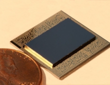
IBM Researchers Simplify Lithography And Reduce Defects In Advanced Chip Fabrication
Researchers at IBM Research – Almaden have found a way to replace a lithography step and provide a significant advantage to mitigate pattern errors and relax design rules in semiconductor fabrication.
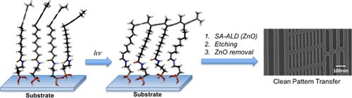
Their work, published recently in Applied Materials & Interfaces, shows a method of selectively depositing a material on feature sizes as small as 15nm by simply growing a film in a selected area.
With traditional methods of fabrication, this would require coating a substrate with resist, patterning the resist through an exposure step, developing the image, depositing an inorganic film and then stripping the resist to give you a patterned inorganic material. The researchers found a way of depositing this inorganic film much more simply, using a self-aligned process, where they immerse a prepatterned substrate in a solution containing a special material and then add that coated substrate it to a deposition chamber.
"We are literally able to grow a component of a device in a controllable manner at the nanoscale," said Rudy J Wojtecki, researcher at at IBM Research – Almaden in Silicon Valley.
It was also found that the selectively deposited ALD film functioned as an effective barrier for isotropic etch chemistries, allowing the selective removal of a metal without affecting the surrounding surface. This work enables selective area ALD as a technology through (1) the development of a material that dramatically reduces defectivity and (2) the demonstrated use of the selectively deposited film as an etch mask and its subsequent removal under mild conditions.

This simple process of self-alignment is one tool required to continue scaling as it promises to simplify complex processes, saving money and reducing errors in final devices.
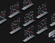
Emerging technologies like AI and neuromorphic computing have very different hardware requirements in comparison to traditional semiconductor processes. IBM's self-alignment process provides an additional tool to fabricate non-traditional hardware that may require three dimensional structures such as cross-point arrays.
The idea of a selective deposition is not new. What is new is the synthesis and demonstration of a new material that enabled the researchers to do this at a scale relevant for the semiconductor industry.
"We’ve primarily drawn from a depth of knowledge in the synthesis of new materials and the ability to tailor a chemical structure for demanding applications. Once we develop methods of scaling this process, we can begin to integrate it as we build next generation hardware, whether it is for new AI hardware or making devices at the 7nm technology node or beyond," Wojtecki added.