Intel, IBM Follow Different Strategies On 14nm FinFET
Intel and IBM presented dueling approaches to the development of FinFET technology for the 14nm technology node during the IEEE International Electron Devices Meeting (IEDM). FinFETs have thin fin-like channels surrounded by multiple gates. This design leads to greater performance and enhanced energy efficiency.
Intel began using FinFET transistors commercially in its "Ivy Bridge" and "Haswell" processors at the 22nm node. The company's second generation of that technology is featured to the new "Broadwell" 14nm chips, which have been released commercially.
Intel has already talked about 14nm FinFETs in September. At IEDM, the company revaled a few new details, such as that it is using "a novel sub-fin doping technique for high performance transistors... and air-gapped interconnects at performance-critical layers."
The sub-fin doping "is achieved through solid-source doping to enable better optimisation of punch-through stopper dopants." The node's 13 copper metal levels use air gapped interconnects "at 80nm and 160nm minimum pitch layers [at levels 4-6 to] provide a 14-17 per cent improvement in capacitance."
Intel increased its use of self-aligned double patterning for critical patterning layers to boost density. But the company did not provide any further details on how it acheived that.
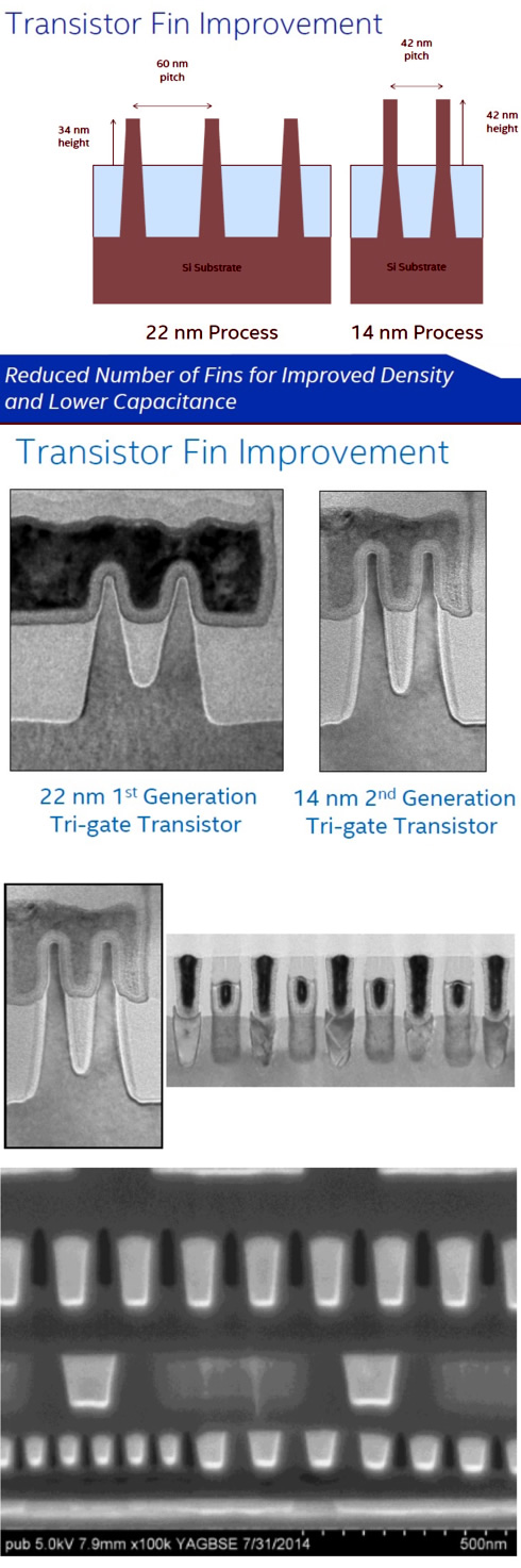
Intel in September disclosed that its 14nm process has the tightest minimum gate pitch in production at 52nm and the highest drive currents yet reported for 14nm technology. The taller, skinnier 14nm finFETs stand 44nm high with a 42nm pitch, compared to 34nm high with a 60nm pitch in Intel's 22nm process.
The result is a node that follows Moore's Law, increases density and slightly improves the rate of reducing cost per transistor.
The company also showcased 14nm 140Mbit SRAM prototype. It memory cell area was just 0.0588 square µm. The provided storage capacity per square mm was 11.6Mbit. Compared to 22nm technology, Intel managed to reduce the silicon area to almost the half.
IBM has optimized its 14nm finFETs both for its high-end Power Server processors as well as for low-power ASICs.
The company said that at 0.8V, the process delivers 35 per cent better performance than IBM's high-performance planar 22nm process. The performance gain stretches over a broad Vt range from 100nA/mm HP FETs to sub-1nA/mm LP and SRAM array FETs, which are featured in many ASICs.
IBM used silicon-on-insulator to deliver the smallest possible embedded DRAM cell for cache memory, in this case measuring just 0.0174mm2. IBM used eDRAM in its 22nm planar node to deliver a Power 8 server CPU that has twice as much L3 cache as Intel's 22nm Haswell server processors, giving Big Blue a performance edge.
A hierarchical back-end process uses 15 levels of copper to support the kind of wiring and power and clock distribution needed for high-end processors and ASICs measuring 600mm2 or more. IBM said the shape and size of finFETs is strategic but did not give further details on the choices it made.