TSMC To Use Different Processes And 3D Packages Across Future Design Platforms
TSMC outlined plans to develop future chips using advanced processes and 3D packaging techniques, tailored for different markets.
Jack Sun, chief technologist and vice president of R&D at TSMC, said in an event in San Francisco that TSMC's will have volume production of its 10nm process before the end of the year and will be ready to take orders for its 7nm process by April. Interestingly, he showed two new variants in the works for InFO stacks -- possibly similar to those Apple is believed to have used for its A10 Fusion SoC.
Dr. Sun also outlined other 3D packaging options for different uses. The new processes and packages will be used for the development of an enhanced mobile platform, design platforms for high performance computing, automotive and the Internet of Things, according to Sun.
The high performance computing platform promises 1V processors running at 3.8 GHz data rates in the 7nm process. The IoT platform will approach near threshold voltages, and the automotive platform will support chips rated to an operating temperature of 150 degrees C.
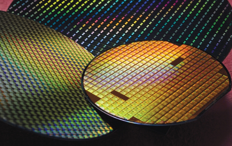
TSMC's 28+ HKMG and 16FF+ processes are in production now, and the 16FFC and 10nm processes are ramping this year. Yields for 256 Mbit SRAMs at 7nm are two months ahead of plan with risk production starting in the first quarter of 2017, said Sun.
The 16nm processes provide about 45% more speed and 80% less leakage than 28+ and support four voltage levels, TSMC said. The 10nm process provides a 50% die scaling and 50% speed gain or 40% power reduction over 16FF+ and provides "the highest density in the industry today in contact pitch," said Sun.
Compared to 10nm, TSMC’s 7nm node delivers 15-20% more speed or 35-40% less power consumption and a 1.63x better routed gate density, said Sun. An ARM Cortex-A72 core in the 7nm process could deliver 30% more performance or 56% less power consumption than in 16FFC.
It could take until the end of 2017 to fully validate in silicon the 7nm process, Hou said. TSMC has more than 20 customers for the 7nm process with multiple tape outs expected before June, said Sun.
Rival Globalfoundries recently announced plans to skip 10nm and move from 14 directly to 7nm.
Intel announced its 10nm process last month, claiming it will be the most dense process in the industry. Observers believe Intel has an edge at 10nm given it is its third-generation FinFET process.
TSMC's R&D manager did not provide much details about TSMC’s 5nm process which it previously announced will ramp in 2020 and use extreme ultraviolet lithography. However, Sun said that the foundry has an EUV stepper with a 125W light source that helped it produce more than 1,400 wafers a day for three consecutive days. However it still requires a 250W version to reach volume production levels. Meanwhile work continues to reduce mask defects, improve resist sensitivity and develop pellicles as well as new metrology tools needed for EUV, Sun said.
In transistors, Sun would not rule out the possibility at 5nm of an advanced FinFET, perhaps using germanium. A gate-all-around design with III-V materials is also possible.
3D packaging
3D packages are becoming key to system integration for delivering smaller parts with higher density.
TSMC produced 2.5D stacks using a silicon interposer to connect multiple die laid on top of it. This approach was applied for the development of Nvidia’s high-end Pascal GPU and its memory.
The so-called CoWoS process is expensive and the resulting components are large, so TSMC developed what it calls InFO for smaller, lower cost parts such as mobile applications processors.
The InFO process and a variant called InFO package-on-package are in production this year, delivering stacks as small as a millimeter in height. A variant called InFO-multidie is in the works. It sports an improved thermal design and can integrate a greater number of logic and memory chips, mainly for mobile systems.
TSMC also described wafer-bonding approaches to 3D packaging for several uses. On approach saves power by integrating CMOS image sensors with image processors and near infrared sensors.
A variant of the process is in the works with partners to stack up to three layers of logic chips into a virtual SoC. The process could form a follow on for either CoWoS or InFO, Sun said.
Another variant of the process geared for RF transceivers is in production at 28nm and will be qualified this year at 16nm. It could also be used to create stacks of sensors, he said.
HPC, IoT And Auto
TSMC is building new platforms for automotive, IoT and high performance computing (HPC).
The foundry aims to have a complete design platform for HPC starting at 7nm. It will sport a new methodology and enable fast interconnect routing, said Hou.
ARM is collaborating on the effort that already involves work on an optimized Cortex-A73 in the 16FFC process that should hit 2.5 GHz next year. At 7nm, chips could approach 4 GHz, he said.
The 7nm version involves a back-end-of-line with lower resistance, new design rules and CoWoS support in 2018.
For IoT, TSMC already has in production ultra low power (UPL) variants of 55, 40 and 28nm processes supporting low supply voltages and leakage. Design of 16 and 7nm ULP variants has started.
Separately, TSMC is qualifying its processes for a wide range of automotive requirements. Sun said the foundry already has ADAS components in production in its 28nm process with tapeouts underway at 20 and 16nm and plans to extend support to 10 and 7nm.