Toshiba Develops High Performance CMOS Device Technology for 20nm Generation LSI
Toshiba today announced that it has developed a breakthrough technology for steep channel impurity distribution that delivers a solution to a key problem for 20nm generation CMOS technology.
The technology opens the door to a future generation of LSI fabricated with bulk CMOS technology, the mainstream technology in today's LSI, by achieving the first practical fabrication process applicable to 20nm generation CMOS devices.
Toshiba unveiled the new technology at the 2009 International Electron Devices Meeting (IEDM) held in Baltimore, Maryland, U.S.A. from December 7 to December 9, one of the semiconductor industry's leading international conferences.
Today's bulk CMOS technology is seen as facing physical limits at around the 20nm generation. Problems such as degradation in electron mobility in the channel area and variation in threshold voltage will become obvious at that scale. These problems can be overcome by realizing a steep impurity distribution in the channel area, a structure that requires a low impurity density surface layer and a high impurity density substrate layer. This structure contributes better gate electrode control over the low-resistance area on the surface by obtaining fine switching of the current.
R&D in steep channel impurity profiles has largely been limited to the partial optimization of nMOS transistors, in which channel impurities easily diffuse, and effective technologies that can secure the overall CMOS performance in the 20nm generation has been a big challenge. As a result, the industry's attention has been directed to new materials or device structures, such as SOI wafers and a 3D gate structure. However, these solutions may result in new process steps that require extra facility investment or that lower productivity. Toshiba's newly developed technology , which is applicable to both the nMOS and pMOS transistors of CMOS devices, opens the way to taking bulk CMOS technology forward to the 20nm generation.
The following technologies are necessary to create a steep channel profile:
(a) A silicon layer formed on the surface of the channel after introducing impurities into the channel area.
(b) A structure that prevents impurity diffusion to the surface due to thermal budget generated during the fabrication process.
(c) Optimization of materials and structures so that the channel functions effectively.
To develop a CMOS device, these technologies are necessary for both the nMOS and pMOS transistors. Although optimization of nMOS has been already achieved, integration of CMOS devices with optimized pMOS has not followed.
Toshiba has extended the nMOS results to develop both nMOS and pMOS devices as shown below. Performance has been confirmed to be 15 to 18% higher than that achieved with the conventional channel structure.
Key points are in the followings;
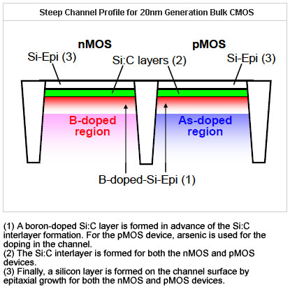
(1) A boron-doped Si:C layer is formed in advance of the Si:C interlayer formation. For the pMOS device, arsenic is used to dope the channel.
(2) An Si:C interlayer is formed for both the nMOS and pMOS devices.
(3) Finally, a silicon layer is formed on the channel surface by epitaxial growth, for both the nMOS and pMOS devices.
Toshiba has optimized both the materials and the structures to realize an efficient fabrication process. Arsenic has been confirmed as a potential candidate for the pMOS channel impurity. In the pMOS device, unwanted fixed charge accumulation in the gate insulator, due to the carbon in the Si:C layer, is resolved by adding a boron-doped silicon layer under the Si:C layer. This result is achieved by making efficient use of the interaction between carbon and boron.
Toshiba unveiled the new technology at the 2009 International Electron Devices Meeting (IEDM) held in Baltimore, Maryland, U.S.A. from December 7 to December 9, one of the semiconductor industry's leading international conferences.
Today's bulk CMOS technology is seen as facing physical limits at around the 20nm generation. Problems such as degradation in electron mobility in the channel area and variation in threshold voltage will become obvious at that scale. These problems can be overcome by realizing a steep impurity distribution in the channel area, a structure that requires a low impurity density surface layer and a high impurity density substrate layer. This structure contributes better gate electrode control over the low-resistance area on the surface by obtaining fine switching of the current.
R&D in steep channel impurity profiles has largely been limited to the partial optimization of nMOS transistors, in which channel impurities easily diffuse, and effective technologies that can secure the overall CMOS performance in the 20nm generation has been a big challenge. As a result, the industry's attention has been directed to new materials or device structures, such as SOI wafers and a 3D gate structure. However, these solutions may result in new process steps that require extra facility investment or that lower productivity. Toshiba's newly developed technology , which is applicable to both the nMOS and pMOS transistors of CMOS devices, opens the way to taking bulk CMOS technology forward to the 20nm generation.
The following technologies are necessary to create a steep channel profile:
(a) A silicon layer formed on the surface of the channel after introducing impurities into the channel area.
(b) A structure that prevents impurity diffusion to the surface due to thermal budget generated during the fabrication process.
(c) Optimization of materials and structures so that the channel functions effectively.
To develop a CMOS device, these technologies are necessary for both the nMOS and pMOS transistors. Although optimization of nMOS has been already achieved, integration of CMOS devices with optimized pMOS has not followed.
Toshiba has extended the nMOS results to develop both nMOS and pMOS devices as shown below. Performance has been confirmed to be 15 to 18% higher than that achieved with the conventional channel structure.
Key points are in the followings;
(1) A boron-doped Si:C layer is formed in advance of the Si:C interlayer formation. For the pMOS device, arsenic is used to dope the channel.
(2) An Si:C interlayer is formed for both the nMOS and pMOS devices.
(3) Finally, a silicon layer is formed on the channel surface by epitaxial growth, for both the nMOS and pMOS devices.
Toshiba has optimized both the materials and the structures to realize an efficient fabrication process. Arsenic has been confirmed as a potential candidate for the pMOS channel impurity. In the pMOS device, unwanted fixed charge accumulation in the gate insulator, due to the carbon in the Si:C layer, is resolved by adding a boron-doped silicon layer under the Si:C layer. This result is achieved by making efficient use of the interaction between carbon and boron.