TSMC Unveils Roadmap to 20nm Process
Taiwan Semiconductor Manufacturing Co Ltd (TSMC) on Thursday outlined its latest developments and process technologies that will be introduced for the 45/40nm, 32/28nm and 22/20nm processes.
Shang-Yi Chiang, the company's SVP of R&D, delivered a lecture at the TSMC 2010 Executive Forum on Leading Edge Technology Feb 24, 2010, in Yokohama, Japan.
Chiang discussed TSMC's 40-nm capacity, yield issues, high-k and lithography. The EE Times web site has posted a transcript of the presentation.
TSMC has been struggling to maintan efficient capacity to catch up with the high demand for 40nm chips. Nvidia and others have delayed their 40nm solutions due to TSMC's low production volume, at least in the early stages. Mr. Chiang said that currently there is just one fab ready to tape production of 40 nanometer, capable of producing about 80,000 (12-inch) wafers per quarter. He added that the company has been working very hard to make up the volume and expects that the production would be doubled by the end of this year.
In addition, Mr. Chang admitted that TSMC had struggled with 40-nm yield issues. However, the problem was resolved in the second half of last year. The defect density was reduced to 0.1-0.3/(inch)2 in the third and fourth quarters of 2009. The number of tape-outs increased at a rapid rate, and half of the taped-out chips are now being mass-produced, TSMC said.
The new technologies introduced for the 45/40nm process are ArF immersion exposure, the third-generation strained silicon and a low-k interlayer insulating film whose dielectric constant was lowered to 2.5.
TSMC has decided to stop its 32-nanometer process addressing all resources on the development of the 28nm process. Risk production for the 28nm low power (LP) SiON process is scheduled for the end of June, Chiang said. The 28LP process will support applications like cellular baseband, application processors, wireless connectivity, and portable consumer electronics.
Also, TSMC will introduce the fourth-generation strained silicon and low-resistance Cu wiring. The company said that it managed to lower the resistance of Cu wiring by improving the flatness of the boundary surfaces of the Cu and barrier metal to prevent electrons flowing on the surface of the wiring from scattering.
As the company outlined last September, SiON gate insulating film is used for the low-power type (28LP) while a high-dielectric gate insulating film and a metal gate electrode (high-k/metal gate) are used for the high-performance type (28HP) and the medium-speed, low-leakage type (28HPL).
Regarding high-k metal gate (28 HP) for the high performance applications, Chang said that it would be introduced in the end of September, followed by the 28PHL in December. This will be the first high-k metal gate introduction for the low power application.
Currently, the yield rate of the 64-Mbit SRAM (28nm) is currently 65% for the 28LP, 27% for the 28HP and 15% for the 28HPL.
Going forward, TSMC plans to introduce 22 nanometer node about two years after we introduce 28 nanometer, sometime in the Q3 of 2012, (high performance). A low power version is expected to be ready in the end of Q1 2013. The company hopes that it would be ready to apply the second generation high-k metal gate for the 20nm process.
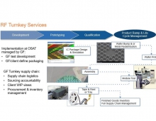
Besides TSMC, IBM and GLOBALFOUNDRIES have initiated researches designed to enable the scaling of semiconductor components to the 22 nanometer node and beyond.
At the 2009 Symposium on VLSI Technology in Kyoto, Japan (June 2009) GLOBALFOUNDRIES reported the first demonstration of a technique that allows the equivalent oxide thickness (EOT) in a high-k metal gate (HKMG) transistor to scale down to well beyond the level required for the 22nm node, while maintaining a combination of low leakage, low threshold voltages, and superior carrier mobility.
Chiang discussed TSMC's 40-nm capacity, yield issues, high-k and lithography. The EE Times web site has posted a transcript of the presentation.
TSMC has been struggling to maintan efficient capacity to catch up with the high demand for 40nm chips. Nvidia and others have delayed their 40nm solutions due to TSMC's low production volume, at least in the early stages. Mr. Chiang said that currently there is just one fab ready to tape production of 40 nanometer, capable of producing about 80,000 (12-inch) wafers per quarter. He added that the company has been working very hard to make up the volume and expects that the production would be doubled by the end of this year.
In addition, Mr. Chang admitted that TSMC had struggled with 40-nm yield issues. However, the problem was resolved in the second half of last year. The defect density was reduced to 0.1-0.3/(inch)2 in the third and fourth quarters of 2009. The number of tape-outs increased at a rapid rate, and half of the taped-out chips are now being mass-produced, TSMC said.
The new technologies introduced for the 45/40nm process are ArF immersion exposure, the third-generation strained silicon and a low-k interlayer insulating film whose dielectric constant was lowered to 2.5.
TSMC has decided to stop its 32-nanometer process addressing all resources on the development of the 28nm process. Risk production for the 28nm low power (LP) SiON process is scheduled for the end of June, Chiang said. The 28LP process will support applications like cellular baseband, application processors, wireless connectivity, and portable consumer electronics.
Also, TSMC will introduce the fourth-generation strained silicon and low-resistance Cu wiring. The company said that it managed to lower the resistance of Cu wiring by improving the flatness of the boundary surfaces of the Cu and barrier metal to prevent electrons flowing on the surface of the wiring from scattering.
As the company outlined last September, SiON gate insulating film is used for the low-power type (28LP) while a high-dielectric gate insulating film and a metal gate electrode (high-k/metal gate) are used for the high-performance type (28HP) and the medium-speed, low-leakage type (28HPL).
Regarding high-k metal gate (28 HP) for the high performance applications, Chang said that it would be introduced in the end of September, followed by the 28PHL in December. This will be the first high-k metal gate introduction for the low power application.
Currently, the yield rate of the 64-Mbit SRAM (28nm) is currently 65% for the 28LP, 27% for the 28HP and 15% for the 28HPL.
Going forward, TSMC plans to introduce 22 nanometer node about two years after we introduce 28 nanometer, sometime in the Q3 of 2012, (high performance). A low power version is expected to be ready in the end of Q1 2013. The company hopes that it would be ready to apply the second generation high-k metal gate for the 20nm process.
Besides TSMC, IBM and GLOBALFOUNDRIES have initiated researches designed to enable the scaling of semiconductor components to the 22 nanometer node and beyond.
At the 2009 Symposium on VLSI Technology in Kyoto, Japan (June 2009) GLOBALFOUNDRIES reported the first demonstration of a technique that allows the equivalent oxide thickness (EOT) in a high-k metal gate (HKMG) transistor to scale down to well beyond the level required for the 22nm node, while maintaining a combination of low leakage, low threshold voltages, and superior carrier mobility.