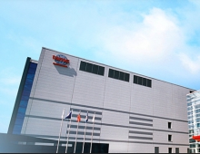
TSMC to Produce Chips Using 28nm Process by early 2010
TSMC , the world's biggest contract chip maker, said on Tuesday it would start using advanced 28-nanometer technology in early 2010 to produce CPUs, graphic processors and chips used in gadgets.
In a highly competitive foundry market, Taiwan Semiconductor Manufacturing Co Ltd (TSMC), United Microelectronics Corp (UMC) and other smaller rivals are racing to develop new process technology for chip production.
The company today unveiled its plans to deliver its 28nm process as a full node technology offering the option of both high-k metal gate (HKMG) and silicon oxynitride (SiON) material to support different customer applications and performance requirements.
The 28nm node will be a full node in TSMC?s manufacturing-flexible 28nm family, so named because it is the only family of processes at these geometries to offer either a HKMG or SiON transistor option.
"Product differentiation, faster time-to-market and investment optimization are the three most important values TSMC delivers to our customers. In support of these values, we are developing this comprehensive 28nm technology family so that it offers choices, depending on the customer applications and performance requirements. " said Jason Chen, vice president, Worldwide Sales and Marketing, TSMC.
The SiON-based 28LPT (low power / high performance) process, the family?s lowest total power and cost-effective technology, is expected to provide twice the gate density, up to 50% more speed or 30-50% lower power consumption than TSMCs? 40LP technology. The 28LPT process is expected to go into initial production in the beginning of 2010 and support applications like cellular baseband, application processors, wireless connectivity, and portable consumer.
TSMC?s decision to build on proven SiON technology for the 28LPT process is driven by changing wireless and portable consumer application dynamics under unrelenting pressure for products to hit market windows, the company said. Consumers a few years ago, wanted low-leakage handsets that supported long battery life. Today?s consumers increasingly rely on their wireless devices for Internet browsing, video streaming, music, mobile TV, GPS navigation, along with traditional phone and texting services. Active usage power consumption is now a much larger factor in battery life.
"SiON gate technology, because of its smaller gate capacitance and therefore lower active power than HKMG, provides a solution with lower total power, cost, and risk for power-limited applications," TSMC said.
"Our customers are really looking for a high performance, low active power, and cost-effective technology to meet their market requirements for their portable consumer products." said Dr. Mark Liu, senior vice president, Advanced Technology Business, TSMC.
The 28HP (high performance) process, TSMC?s first HKMG technology, will support performance-demanding applications such as CPU, graphic processors, and FPGAs with twice the gate density and over 30% higher speed than TSMC?s 40G process at similar power density, TSMC added.
Going forward, the HKMG technology is very promising for device scaling at even smaller geometries beyond 28nm. The 28HP process is expected to enter initial production in the first half of 2010. TSMC?s 28nm technologies are currently supported by alpha version design kits. The 28nm CyberShuttle, a prototyping service, will begin near the end of 2008 and features competitive cycle time and frequency. TSMC, which counts Texas Instruments and Nvidia among its major clients, has been driving process technology to advanced 90-, 65- and 45-nanometer. The company has been also believed to apply its 40nm process to chips manufactured for AMD, according to recent reports.