IBM Researchers Talk About the Future of EUV at SPIE
IBM is committed to extending the Extreme ultraviolet (EUV) patterning technology to its limits, and papers at this week's 2018 International Society for Optics and Photonics (SPIE) Advanced Lithography conference will show how much the technology can be extended to the 5nm, 3nm, and future nodes.
The latest POWER9 technology by IBM is based on the 14nm logic technology developed at IBM Research earlier this decade. But IBM continues to push the boundaries of advanced logic nodes.
For both the 7nm and 5nm nodes, IBM and its alliance partners at the SUNY Poly Colleges of Nanoscale Science and Engineering in Albany, NY relied heavily on transistor and interconnect patterning driven by Extreme Ultraviolet (EUV) lithography.
IBM and its development partners are fully committed to extending EUV patterning technology to its limits, and five papers at this week's SPIE Advanced Lithography conference will examine EUV patterning, all aspects of equipment, materials, and process needed to be explored to their limits.
This exploration starts with the fundamental variability of ASML's EUV lithography system, with which IBM now has four years of experience. In the paper "Characterization and control of EUV scanner dose uniformity and stability," Chris Robinson fully characterizes the exposure stability of a pre-manufacturing EUV system and shows that although its exposure control is far from perfect, proper characterization and control techniques can improve performance.
Extending EUV lithography to its fullest potential will require revisiting some of the oldest assumptions of the lithography process itself. In the paper "Aqueous developers for ultrathin chemically amplified EUV resists," Dario Goldfarb dives into the fundamental physical and chemical process of lithography to show potential new pathways forward to high-contrast imaging. In this manner, he opens the proverbial "black box" of the lithography development process and thus gives new life to current patterning materials to extend beyond the 5nm node.
Further frontiers in patterning will depend on advancements in patterning materials, and two talks, "Polymer brush as adhesion promoter for EUV patterning" by Jing Guo and "Silicon-based hardmask development for EUV patterning" by Anuja De Silva, add vital tools to the patterning toolbox. Both of these talks highlight the results of years of materials work in patterning films by IBM engineers, as well as collaborative efforts with many critical vendors in the semiconductor industry. IBM believes that the results of this invention, characterization, and collaboration fully enable EUV patterning at the dimensions necessary for the 5nm and 3nm nodes.
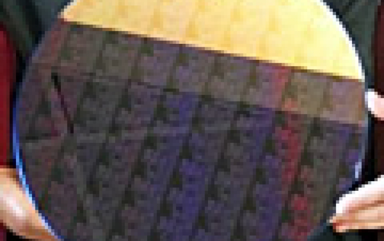
Achieving patterning yields that are compatible with bleeding-edge logic manufacturing is a complex feat. Luciana Meli, in "Defect detection strategies and process partitioning for single expose EUV patterning," ties together many of the concepts discussed above to show how to measure, understand, and improve upon the factors that drive semiconductor process yield at dimensions that are no wider than a few stands of DNA, with perfection over a 12-inch wafer.