TSMC Says Quad Patterning Could Be Needed For 10nm
Quad patterning may be needed for 10nm manufacturing process technology if extreme ultraviolet (EUV) lithography is not ready in 2015, TSMC says.
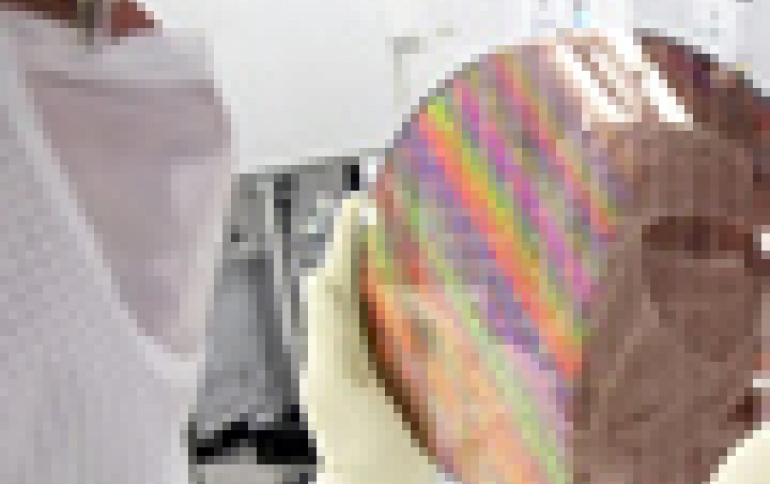
In an interview with EE Times after a keynote at the ARM TechCon, TSMC's chief technologist Jack Sun said that quad patterning, which involves four passes through a lithography stepper using four different masks, was one of several options TSMC is exploring as it works on path finding for the process.
Multiple patterning means increased wafer costs, although the cost could be offset by the improved transistor density.
Intel is also considering using quadruple patterning for some mask layers, although the company has already invested in ASML Holding NV, Europe's largest semiconductor equipment maker, to drive extreme ultraviolet (EUV) lithography forward.
EUV lithography hasbeen long seen as the inevitable successor to optical immersion lithography.
Intel plans to start production of chips in the process in three years. Intel also expects to use double patterning in some layers of some chips at 14 nm, which are expected before the end of next year.
In his keynote, TSMC's Sun also showed the roadmap for TSMC, which includes starting limited test production of 20nm planar chips by the end of the year and a 16nm FinFET process starting test production late next year. TSMC expects the new 20nm process holds traditional advances of as much as 35 per cent in performance and power capabilities.