Intel's Aims At 7nm Process Technology by 2017
Intel has outlined its semiconductor process roadmap at its 9th annual Research@Intel press event this week. By focusing on research & development and with investments in production, the company believes that technology innovation will shrink the chip making process down to 7nm in 6 years from now.
Mike Mayberry, Director of Components Research VP, Technology and Manufacturing Group at Intel unveiled the company's semiconductor technology road map. Intel seems to remain on pace with its ambitious product and manufacturing cadence referred to as the company's "tick-tock" strategy. That plan revolves around introducing an entirely new processor microarchitecture alternating with a cutting edge manufacturing process about every 12 months.
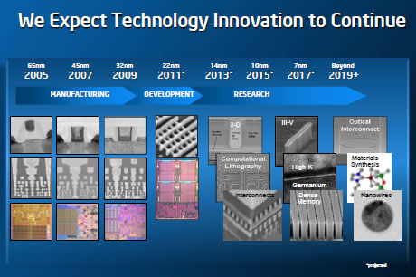
Intel is currently developing its 22nm process. For the first time, transistors using a three-dimensional structure will be put into high-volume manufacturing at the 22nm node in an Intel chip codenamed "Ivy Bridge." The new chip is slated for high-volume production readiness by the end of this year. The 22-nm Ivy Bridge chips are in the "tick" side of the product introduction cycle that Intel has delivered six times going back to 65-nm.
Two years later, manufacturing at the 14nm node is expected to kick-off, followed by a further progress in 10nm in 2015. Finally in 2017, Intel plans to proceed with the first 7nm chips.
In order to ensure these steps forward, Intel's research focus for the next few years will be related to 3-D tri-gate transistors, III-V group compound, optical interconnection lithography, high-K germanium, materials synthesis, high-density memory, nanowires, and more.


Concluding, Mike Mayberry descridbed Moore's Law as "an expectation of continued innovation" and underlined Intel's continous focus on research, rapid development and investments in production. He added that the scaling research is more about materials research and that solving problems will bring new opportunities.
Intel is currently developing its 22nm process. For the first time, transistors using a three-dimensional structure will be put into high-volume manufacturing at the 22nm node in an Intel chip codenamed "Ivy Bridge." The new chip is slated for high-volume production readiness by the end of this year. The 22-nm Ivy Bridge chips are in the "tick" side of the product introduction cycle that Intel has delivered six times going back to 65-nm.
Two years later, manufacturing at the 14nm node is expected to kick-off, followed by a further progress in 10nm in 2015. Finally in 2017, Intel plans to proceed with the first 7nm chips.
In order to ensure these steps forward, Intel's research focus for the next few years will be related to 3-D tri-gate transistors, III-V group compound, optical interconnection lithography, high-K germanium, materials synthesis, high-density memory, nanowires, and more.
Concluding, Mike Mayberry descridbed Moore's Law as "an expectation of continued innovation" and underlined Intel's continous focus on research, rapid development and investments in production. He added that the scaling research is more about materials research and that solving problems will bring new opportunities.