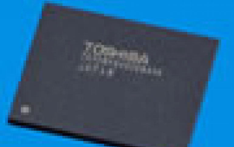
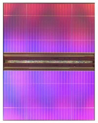
Toshiba Develops Highest Density Non-volatile RAM
Toshiba today announced the prototype of a new FeRAM
?Ferroelectric Random Access Memory? that redefines industry
benchmarks for density and operating speed.
The new chip realizes storage of 128-megabits and read and
write speeds of 1.6-gigabytes a second, the most advanced
combination of performance and density yet achieved. Full
details of the new FeRAM will be presented this week at the
International Solid-State Circuits Conference 2009 (ISSCC2009)
in San Francisco, USA.
 The new FeRAM modifies Toshiba's original chainFeRAM
architecture, which contributes to chip scaling, with a new
architecture that prevents cell signal degradation, the usual
tradeoff from chip scaling. The combination realizes an
upscaled FeRAM with a density of 128-megabit. Furthermore, a
new circuit that predicts and controls the fluctuations of
power supply supports high-speed data transfers. This allowed
integration of DDR2 interface to maximize data transfers at a
high throughput at low power consumption, realizing read and
write speeds of 1.6 gigabytes a second. In developing the new
FeRAM, Toshiba broke its own record of 32-megabit density and
200-megabit data transfers, pushing performance to eight times
faster than the transfer rate and density of the previous
records and the fastest speed of any non-volatile RAM.
The new FeRAM modifies Toshiba's original chainFeRAM
architecture, which contributes to chip scaling, with a new
architecture that prevents cell signal degradation, the usual
tradeoff from chip scaling. The combination realizes an
upscaled FeRAM with a density of 128-megabit. Furthermore, a
new circuit that predicts and controls the fluctuations of
power supply supports high-speed data transfers. This allowed
integration of DDR2 interface to maximize data transfers at a
high throughput at low power consumption, realizing read and
write speeds of 1.6 gigabytes a second. In developing the new
FeRAM, Toshiba broke its own record of 32-megabit density and
200-megabit data transfers, pushing performance to eight times
faster than the transfer rate and density of the previous
records and the fastest speed of any non-volatile RAM.
FeRAM combines the fast operating characteristics of DRAM with flash memory's ability to retain data while powered off, attributes that continue to attract the attention of the semiconductor industry. Toshiba said that it would continue R&D in FeRAM, aiming for further capacity increases and eventual use in a wide range of applications, including the main memory of mobile phones, mobile consumer products, and cache memory applications in products such as mobile PCs and SSDs.
In the earlier generation of 64-megabit FeRAM employed a data-line design in which neighboring data-lines operated in sequence: one is off when the other is on. This allowed off lines to provide a noise barrier between on lines, contributing to chip scaling and fine performance. Previous chain architecture collected four data-lines but Toshiba has successfully increased the number of data-lines to eight, which led to a decrease in the total chip area.
Chip scaling causes signal degradation as the stored polarization of memory cell gets smaller. By shortening the data-line pitch and using chain architecture to decrease the number of memory cells connecting to sense amplifiers , Toshiba maintained the same cell signal level without any chip area penalty. Furthermore, improvement of the sensing technique reduced the parasitic capacitance and realized a reading signal of 200mV, sufficient for practical application.
A circuit that can predict power fluctuation during read/write and control the power supply was also added. This new circuit realizes the voltage required for read and write, allowing the new FeRAM to add a DDR2 interface and opening the way to practical use.
Main specifications:
Process 130 nanometer CMOS
Density 128 megabits
Cell size 0.252 μm2
Read/ write speed (bandwidth) 1.6 gigabytes/second (DDR2 interface)
Cycle time 83 nanoseconds
Access time 43 nanoseconds
Power supply 1.8V
At the same event, Intel announced its latest developments in the SRAM memory. The company said that it has made an SRAM memory prototype with a density of 291 Mbits using the 32nm technology.
NEC also announced 32Mbit MRAM prototypes.