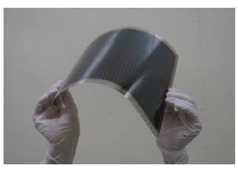
New Energy and Industrial Technology Development Organization (NEDO) and Toshiba have developed the world's largest film-based perovskite photovoltaic module.
The module is 703cm2 (24.15 x 29.10cm) and realizes a power conversion efficiency (PCE) of 11.7%, overcoming the difficulties of increasing size and efficiency at the same time.
The module was developed using the meniscus printing technology owned by Toshiba and a newly developed printing process. Toshiba developed the printing process for a larger module by controlling the chemical reaction between PbI2 and MAI on the substrate, using the ink composition as a mechanism. The company has also improved the uniformity of the layer thickness and increased the homogeneity of the crystal layer properties over a larger area, by controlling the process and adjusting the perovskite crystal growth conditions during the printing process. As a result, a PCE of 11.7% has been obtained on a module with an area of 703cm2, almost as large as 900cm2, the practical a scale. It is a step closer to practical application.

Alongside the advantages in terms of size and efficiency, Toshiba expects that the flexibility and the lightness of the module to open up possibilities for use in a wide range of locations.
NEDO and Toshiba plan to continue work to enlarge the module and to boost its efficiency to that of crystal silicon photovoltaic modules by improving the printing technology and materials used in the perovskite layer. The ultimate goal is to achieve photovoltaic modules with a levelized cost of electricity of 7 yen per kWh by 2030.