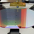
Samsung Electronics' Foundry Business has commenced mass production of System-on-Chip (SoC) products built on its second generation 10-nanometer (nm) FinFET process technology, 10LPP (Low Power Plus).
Samsung claims that its 10LPP process technology allows up to 10-percent higher performance or 15-percent lower power consumption compared to its first generation 10nm process technology, 10LPE (Low Power Early).
SoCs designed with 10LPP process technology will be used in digital devices scheduled to launch early next year and are expected to become more widely available throughout the year. Market experts anticipate Qualcomm's next-gen flagship chipset Snapdragon 845 and Samsung's Exynos 9 series application processors will adopt the SoC products built on the new 10LPP technology.
Samsung also announced that its newest manufacturing line, S3, located in Hwaseong, Korea, is ready to ramp up production of process technologies including 10nm and below. The company is considering rolling out a next-generation DRAM using an early 10nm process as early as the beginning of 2019. Samsung's 7nm FinFET process technology with EUV (Extreme Ultra Violet) will also be mass produced at S3. Samsung Electronics's Hwaseong Semiconductor Complex boasts not only DRAM and NAND flash but foundry (semiconductor production consignment) lines.
S3 is the third fab of Samsung's Foundry Business, following S1 in Giheung, Korea and S2 in Austin, USA.
EUV exposure equipment is used for a 7nm foundry process, but some can be used for DRAM production. However, as the wafer production speed of the 10nm micro process is slower than the current patterning photo process, the key is whether or not Samsung Electronics will be able to find a way to profitability.
Currently, exposure equipment that draws semiconductor circuit lines uses 193nm ArF excimer laser and liquid immersion and can draw a physically maximum 38nm circuit linewidth only at one time. In order to overcome the linewidth problem, semiconductor engineers strengthened the micro process to draw circuit lines by dividing circuit patterns two or three times but it is generally said that it is difficult to realize 10nm or less nm DRAMs. EUV exposure equipment can significantly reduce circuit linewidth by using 13.5 nm light waves shorter than visible rays, thus enabling a 10nm or less nm micro process.
Samsung Electronics has been using a double-quad patterning process which overlaps circuits multiple times with existing exposure equipment to mass-produce 18-nm or less precise DRAMs since October of last year.
Samsung's competitors such as SK Hynix is planning to begin late-10-nm DRAMs in the fourth quarter of this year, and complete researching and developing a mid-10-nm DRAM in the latter half of next year. However, SK Hynix has not disclosed anything related to EUV exposure equipment.
Samsung and Qualcomm are cooperating on an 8-nanometer process, which will likely roll out commercially next year.
Samsung was the first in the industry to begin mass production of chips based on 10nm process in October 2016 and completed developing 8 nm processing technology last month. TSMC produces chips at 10nm process technology and has announced that it will introduce the next-generation 7nm processing technology.