
Today AMD unveiled preliminary details of its forthcoming GPU architecture, Vega. Conceived and executed over 5 years, Vega architecture enables new possibilities in PC gaming, professional design and machine intelligence.
The Vega architecture's memory subsystem enables GPUs to address very large data sets spread across a mix of memory types. The high-bandwidth cache controller in Vega-based GPUs can access on-package cache and off-package memories in a flexible, programmable fashion using fine-grained data movement.

The Vega architecture enables a new memory hierarchy for GPUs. This radical new approach comes in the form of a new high-bandwidth cache and its controller. The cache features HBM2 technology which is capable of transferring terabytes of data every second, doubling the bandwidth-per-pin over the previous generation HBM technology. HBM2 also enables much greater capacity at less than half the footprint of GDDR5 memory. Vega architecture is optimized for streaming very large datasets and can work with a variety of memory types with up to 512TB of virtual address space.

While HBM1 stacked topped out at 1GB each, which means Fiji could have no more than 4GB of VRAM. HBM2 stacks go much higher - up to 8GB per stack - which means AMD's memory capacity problems when using HBM have for all practical purposes gone away. AMD could in time offer 8GB, 16GB, or even 32GB of HBM2 memory, which is more than competitive with current GDDR5 memory types.


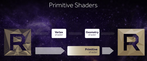
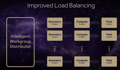
Today's games and professional applications make use of incredibly complex geometry enabled by the extraordinary increase in the resolutions of data acquisition devices. The hundreds of millions of polygons in any given frame have meshes so dense that there are often many polygons being rendered per pixel. Vega's next-generation geometry pipeline enables the programmer to extract efficiency in processing this complex geometry, while also delivering more than 200% of the throughput-per-clock over previous Radeon architectures. It also features improved load-balancing with an intelligent workload distributor to deliver consistent performance.
At the core of the Vega architecture is a new, next-generation compute engine built on flexible compute units that can natively process 8-bit, 16-bit, 32-bit or 64-bit operations in each clock cycle. These compute units are optimized to attain significantly higher frequencies than previous generations and their support of variable datatypes makes the architecture highly versatile across workloads.
AMD's new architecture will also add support for what AMD calls the Draw Stream Binning Rasterizer, which true to its name, will give Vega the ability to bin polygons by tile. By doing so, AMD will cut down on the amount of memory accesses by working with smaller tiles that can stay-on chip. This will also allow AMD to do a better job of culling hidden pixels, keeping them from making it to the pixel shaders and consuming resources there.
Vega is designed to handle up to 11 polygons per clock with 4 geometry engines, according to AMD.
AMD has also significantly reworked how the ROPs interact with their L2 cache. Starting with Vega, the ROPs are now clients of the L2 cache rather than the memory controller, allowing them to better and more directly use the relatively spacious L2 cache.
Based on what we know so far, Vega stands to be the biggest change to AMD's GPU architecture since GCN 1.0 was released 5 years ago, and the changes to the ALUs, the ROPs, the memory structure, and other aspects of Vega reinforce this notion.
GPU products based on the Vega architecture are expected to ship in the first half of 2017.