 The semiconductor industry relies on perpetual miniaturization, and for this to continue requires a holistic approach to the lithography process and a UV lithography ready for volume manufacturing - the latter is not so far away according to ASML.
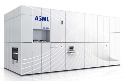
Speaking at last week's SPIE Advanced Lithography conference in San Jose, Dutch ASML, which is developing EUV machines for the semiconductor industry, said that its machines will soon be capable of using a a light source bright enough to pattern chips cheaply.
EUV refers to the light source that is used in the lithography machine. Since lithography is an optical technology, one of the things that limits the resolution of the equipment is the wavelength of the light that is used. Shortening the wavelength of the light means higher resolution and smaller features.
ASML's technology uses 13.5-nanometer light instead of today’s 193-nanometer light and could allow chipmakers to create finer features without having to expose chips multiple times, a process that can add significantly to the expense of the manufacturing process. So ASML claims that EUV has an advantage over Double Patterning, because it does not increasethe amount of lithography exposures per wafer.
Until recently, the dimness of the EUV light source has been limiting EUV’s prospects. ASML said it has pushed the limit of that light source to 200 W and aims to reach 250 W by the end of the year.
The company has long targeted 250 watts as the brightness needed for chipmakers to adopt the technology for high-volume production.
The brighter the light source, the less time it needs to pattern a chip. ASML says that a 250W source will allow for making more than 125 wafers per hour, and more than 1500 wafers per day, as the system's availability has been demonstrated to be higher than 80%.
The challenge going forward will be to get the machines to run at high power nearly all the time. A number of customers, including Intel and TSMC, are testing EUV tools at lower power in their fabs, and those machines are producing wafers 70 to 80 percent of the time. But that’s still short of the performance of today’s 193-nm machines, which aim for 95 percent availability, 24-7.
But in order to consider EUV succesful, a number of other components in the lithographic process should be improved: masks that carry the patterns to be printed on a wafer; protective "pellicles" that guard those masks against contamination; and the photo-sensitive resists that the light must ultimately shine on and chemically transform in order to transfer a pattern to a wafer.
ASML says EUV machines could be part of high-volume chip manufacturing around 2018. Currently, TSMC plans to start using the technology at the 7-nanometer node, which is set for that time. The company anticipates adopting EUV for high-volume manufacturing at the 5-nanometer node, which would happen around 2020.