 Intel today disclosed details of its newest microarchitecture that is optimized with its 14nm manufacturing process.
Intel disclosed details of the microarchitecture of the Intel Core M processor, the first product to be manufactured using 14nm. The company says that the new microarchitecture along with the advanced manufacturing process will contribute to smaller, cooler and more silent devices.
Intel today disclosed details of its newest microarchitecture that is optimized with its 14nm manufacturing process.
Intel disclosed details of the microarchitecture of the Intel Core M processor, the first product to be manufactured using 14nm. The company says that the new microarchitecture along with the advanced manufacturing process will contribute to smaller, cooler and more silent devices.
Intel architects and chip designers have achieved greater than two times reduction in the thermal design point when compared to a previous generation of processor while providing similar performance and improved battery life.
Intel's first 14nm technology in volume production uses second-generation Tri-gate (FinFET) transistors.It will be used to manufacture a wide range of high-performance to low-power products including servers, personal computing devices and Internet of Things.
The first systems based on the Intel Core M processor will be on shelves for the holiday selling season followed by broader OEM availability in the first half of 2015.

Intel wants a greater foothold in the mobile market. And with Broadwell-Y they believe they finally have what they need to accomplish that goal.

Let's start with some information about Broadwell's GPU. Generally,
Broadwell’s GPU is a continuation of the Intel Gen7 architecture first seen in Ivy Bridge. While there are some changes, this is still the same GPU architecture that we’ve seen from Intel for the last two generations.
Broadwell’s GPU has been upgraded to support the latest graphics APIs -- Direct3D feature level 11_2 and Direct3D 12 -- meaning Intel will not longer lag behind Nvidia's and AMD's offerings.

Intel has confirmed that Broadwell’s GPU will offer support for OpenCL 2.0, including OpenCL’s shared virtual memory.
Broadwell-Y, like Haswell-Y before it, implements a single slice configuration of Intel’s GPU architecture. However the composition of a slice will be changing for Broadwell, and this will have an impact on the balance between various execution units.

Intel isn’t talking about overall GPU performance, at least for now.
The company is reiterating the benefits of their 14nm process, noting that because 14nm significantly reduces GPU power consumption it will allow for more thermal headroom, which should further improve both burst and sustained GPU performance in TDP-limited scenarios relative to Haswell.
Broadwell’s GPU also brings the 'Duty Cycle Control'. The idea is to extract more idle power gains. Transistors require a minimum voltage to operate, which means that after a certain point Intel can no longer scale down their voltage and reduce the poewr consumption further. Intel’s solution to this problem is is to start turning off the GPU instead -- the process of duty cycling. By putting the GPU on a duty cycle Intel can run the GPU for just a fraction of the time – down to 12.5% of the time – which gets around the threshold voltage issue entirely.Control of the duty cycle is then handled through a combination of the GPU hardware and Intel’s graphics drivers.
Duty cycle control is especially important for the TDP and battery life constrained Y SKU, but ultimately all mobile SKUs would stand to benefit from this feature.
Intel is also upgrading their GPU’s media capabilities for Broadwell. The increase in sub-slices and the resulting increase in samplers will have a direct impact on the GPU’s video processing capabilities – the Video Quality Engine and QuickSync – further increasing the throughput of each of them, up to 2x in the case of the video engine. Intel is also promising quality improvements in QuickSync.
Broadwell’s video decode capabilities will also be increasing compared to Haswell. On top of Intel’s existing codec support, Broadwell will be implementing a hybrid H.265 decoder, although the shaders will be also used for decoding, making it less power efficient than doing everything in hardware.

last but not least, Broadwell’s display controller will be updated and will support HDMI 1.4 and DP 1.2/eDP 1.3a. The Y SKU will also is get native support for 4K, although you should not expect Broadwell-Y to have the performance necessary to do intensive rendering at this resolution.
Regarding Broadwell’s CPU architecture, Intel is shooting for a better than 5% IPC improvement over Haswell.
In order to deliver that IPC increase Intel will be relying on architectural tweaks in Broadwell: Bigger schedulers and buffers for better feed of the CPU cores. Broadwell’s out-of-order scheduling window for example is being increased to allow for more instructions to be reordered, thereby improving IPC. Meanwhile the L2 translation lookaside buffer (TLB) is being increased from 1K to 1.5K entries.
The TLBs are also receiving some broader feature enhancements that should again improve performance. A second miss handler is being added for TLB pages, allowing Broadwell to utilize both handlers at once to walk memory pages in parallel.
Meanwhile, Broadwell’s branch predictor will see its address prediction improved for both branches and returns, allowing for more accurate speculation of impending branching operations.
In addition, both multiplication and division are receiving a performance boost thanks to performance improvements in their respective hardware. Floating point multiplication is seeing a sizable reduction in instruction latency from 5 cycles to 3 cycles, and division performance is being improved by the use of a Radix-1024 (10bit) divider. Even vector operations will see some improvements here.
Finally, Intel is once again targeting cryptography for further improvements.
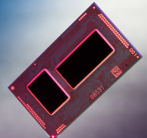
Specifically for the Core M, Intel has made a number of alterations to everything from the CPU packaging to the process node itself.
Intel's biggest goal with Core M is to offer a processor for 10" tablets under with 10mm in thickness that are passively cooled - -a device that would require a sub-5W SoC. In addition, the Core M variant is designed to further reduce power consumption by optimizing the resulting transistors for lower power, lower voltage, lower clockspeed operation. By doing this Intel was able to further reduce power consumption in all of the major areas over what would be a traditional 14nm Intel process.


In the resulting 14nm Broadwell-Y process, voltage, capacitance, and leakage were all improved over the traditional 14nm process. Capacitance was reduced by 15%, minimum operating voltages by 10%, and leakage was improved to the point that it reduced SoC power consumption by 10%.
Meanwhile Broadwell-Y’s on-package PCH has also received its own optimizations to reduce power consumption on the SoC’s total power consumption. Although the PCH itself is still made on Intel’s 32nm process, it has seen optimizations that cut its idle power consumption by 25% and its active power consumption by 20%.

Feeding all of that silicon is Intel’s second generation Fully Integrated Voltage Regulator (FIVR), which is more efficient.
The final element of Intel’s power optimization efforts involves further adjustments to turbo boost. New for Broadwell-Y is a 3rd power state, PL3, which allows for even greater turbo boosting, but for only some milliseconds. PL3 represents the maximum amount of power the device battery can deliver.
The final element of Intel’s fanless challenge is the size of the SoC itself. Intel has focused on making Broadwell-Y the smallest Core processor yet, making the entire SoC under 500mm2 in size.
At 82mm2 the Broadwell-Y CPU die is some 37% smaller than the Haswell-Y CPU die, none the less packing a dual-core CPU and a full GPU slice.
Haswell-Y’s already small ball pitch of .65mm was further reduced to just .5mm, producing a package with Intel’s smallest solder ball pads yet.

Intel has also made a number of changes for Broadwell-Y to reduce the Z-height of the Y SoCs, as even 1.5mm for the SoC starts to become a significant design constraint in a sub-10mm device. The Z-height of the Broadwell-Y die itself is down to 170um. Meanwhile the Z-height of the substrate has been cut in half from 400um to 200um.
Last but not least, Intel’s 3DL inductors are on their own PCB on the back of the SoC, extending well below the back of the package.
All told then, the combination of these space optimizations has reduced Broadwell-Y’s Z-height by nearly 30%, from 1.5mm on Haswell-Y to 1.04mm on Broadwell-Y.