
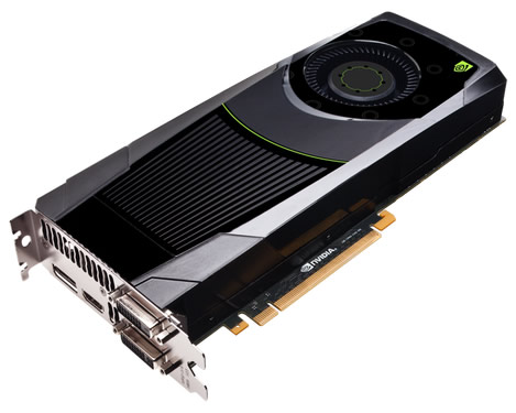
The next generation GeForce GTX 680 GPU has arrived,based on the company's latest GPU architecture, codenamed "Kepler".
 NVIDIA’s Kepler architecture builds on the foundation first established in 2010 with NVIDIA's Fermi GPU architecture. Fermi introduced an entirely new parallel geometry pipeline optimized for tessellation and displacement mapping. Kepler continues to provide great tessellation performance and combines this with new features.
The first GPU based on our new Kepler architecture, codenamed "GK104," is Nvidia's highest performing GPU todate, it is also the most efficient in terms of power consumption. GK104 is fabricated on an optimized 28nm process, and every internal unit was designed for the best perf/watt possible. The first product being introduced based on GK104 is the GeForce GTX 680.
Here are the specs and a comparison with Nvidia's previous GPUs:
| |
GTX 680 |
GTX 580 |
GTX 560 Ti |
GTX 480 |
| Stream Processors |
1536 |
512 |
384 |
480 |
| Texture Units |
128 |
64 |
64 |
60 |
| ROPs |
32 |
48 |
32 |
48 |
| Core Clock |
1006MHz |
772MHz |
822MHz |
700MHz |
| Shader Clock |
N/A |
1544MHz |
1644MHz |
1401MHz |
| Boost Clock |
1058MHz |
N/A |
N/A |
N/A |
| Memory Clock |
6.008GHz GDDR5 |
4.008GHz GDDR5 |
4.008GHz GDDR5 |
3.696GHz GDDR5 |
| Memory Bus Width |
256-bit |
384-bit |
256-bit |
384-bit |
| Frame Buffer |
2GB |
1.5GB |
1GB |
1.5GB |
| FP64 |
1/24 FP32 |
1/8 FP32 |
1/12 FP32 |
1/12 FP32 |
| TDP |
195W |
244W |
170W |
250W |
| Transistor Count |
3.5B |
3B |
1.95B |
3B |
| Manufacturing Process |
TSMC 28nm |
TSMC 40nm |
TSMC 40nm |
TSMC 40nm |
| Price |
$499 |
$499 |
$249 |
$499 |
The GeForce GTX 680 GPUs are featuring Nvidia's new SMX streaming multiprocessors and NVIDIA technologies like
TXAA, FXAA, Adaptive VSync and GPU Boost. Let's see some information about these new features.
In order to reduce power consumption while still improving GPU performance, Nvidia has eliminated the shader clock and significantly increased the number of CUDA Cores, Special Function Units, and texture units. Kepler’s new Streaming Multiprocessor, called "SMX", runs at graphics clock rather than 2x graphics clock; but with 1536 CUDA cores in GK104, the GeForce GTX 680 SMX provides 2x the performance per watt of Fermi’s SM (GF110). This allows the GeForce GTX 680 to deliver greater performance/watt when compared to GeForce GTX 580.
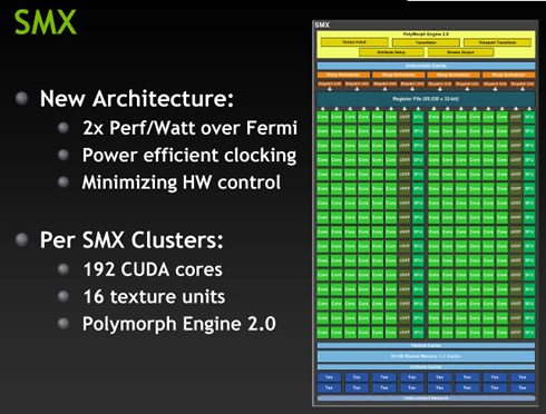
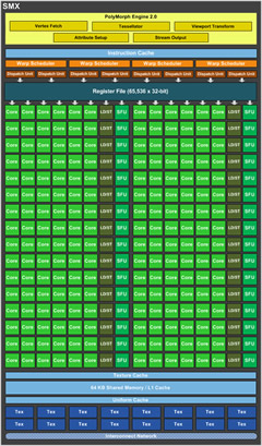
The GeForce GTX 680 GPU consists of four GPCs, eight next-generation Streaming Multiprocessors (SMX), and four memory controllers. Each GPC has a dedicated raster engine and two SMX units. With a total of eight SMX units, the GeForce GTX 680 implementation has 1536 CUDA Cores.
The SM’s CUDA cores perform pixel/vertex/geometry shading and physics/compute calculations. Texture units perform texture filtering and load/store units fetch and save data to memory. Special Function Units (SFUs) handle transcendental and graphics interpolation instructions.
Finally, the PolyMorph Engine handles vertex fetch, tessellation, viewport transform, attribute setup, and stream output.The final SMX unit to receive significant modifications in Kepler is the PolyMorph Engine. GeForce GTX 680 contains 8 PolyMorph Engines, compared to 16 for GeForce GTX 580; however, the Kepler PolyMorph engine was redesigned to deliver roughly double the per-clock performance of the Fermi version. GeForce GTX 680’s 30% higher shipping clock speed promise to offer a significant overall improvement in tessellation workloads.

GeForce GTX 680’s memory subsystem was also completely revamped, resulting in higher memory clock speeds,operating at 6008MHz data rate.Tied to each memory controller are 128KB L2 cache and eight ROP units (each of the eight ROP units processes a single color sample). With four memory controllers, a full GeForce GTX 680 GPU has 512KB L2 cache and 32 ROPs (i.e., 32 color samples).
 |
 |
Nvidia Polymorph engine 2.0 |
Kepler block diagram |
The following table provides a high-level comparison of Kepler vs. previous generation NVIDIA GPUs:
To improve performance even further, GeForce GTX 680 also features new GPU Boost technology that automatically increases the graphics clock speed to maximize frame rate in games. In cases where the GPU isn’t fully taxed, it would be beneficial if the GPU could increase its clock frequency to deliver improved 3D performance and/or higher image quality with richer graphics effects enabled. This is where NVIDIA’s GPU Boost technology comes in: a combination of hardware and softwarem technology that works with the GeForce GTX 680, GPU Boost works in the background, dynamically adjusting the GPU’s graphics clock speed automatically, based on GPU operating conditions. Dedicated hardware circuitrycontinually monitors GPU power consumption.
170W is the typical board power NVIDIA has defined for the GeForce GTX 680 and GPU Boost. Under load, most cards will typically operate at this power level. Nvidia ultimately determined this power level delivers the optimal combination of GPU power, temps, and acoustics.
GPU Boost operates completely autonomously with no game profiles and no intervention required by the end user.
GeForce GTX 680’s base 3D frequency is 1006MHz, which is called the "Base Clock." This is the minimum 3D frequency the GPU is guaranteed to achieve running under load in TDP apps (strenuous real-world applications that push power utilization to the Thermal Design Power limits of a GPU).
The "Boost Clock" is the average clock frequency the GPU will run under load in many typical non-TDP apps that require less GPU power consumption. On average, the typical Boost Clock provided by GPU Boost in GeForce GTX 680 is 1058MHz, an improvement of just over 5%. The Boost Clock is a typical clock level achieved while running a typical game in a typical environment.
However, in many cases the GPU will have additional power headroom available and will automatically increase the Boost Clock even higher than 1058MHz. As long as the GPU remains under its power target, GPU Boost will increase the GPU Clock: clock speeds of 1.1GHz or higher have been observed internally in testing various non-TDP apps.
GPU Boost is fully compatible with GPU overclocking. Using third-party overclocking utilities provided by NVIDIA board partners, GeForce GTX 680 users can adjust the GPU’s power target to enable higher clock speeds.
Once the power target has been increased, the GPU can be overclocked by raising the GPU clock offset.
GeForce GTX 680 also supports a number of other features:
NVIDIA Adaptive VSync technology dynamically turns VSync on and off as needed for reduced tearing and stutter.
NVIDIA FXAA technology is now coming to the GeForce GTX 680’s driver control panel. NVIDIA FXAA technology harnesses the power of the GPU’s CUDA Cores to reduce visible aliasing. FXAA is a pixel shader-based image filter that is applied along with other post processing steps like motion blur and bloom. For game engines making use of deferred shading, FXAA provides a performance and memory advantage over deferred shading with multi-sample anti-aliasing (MSAA). FXAA targets edge aliasing and also aliasing on single-pixel and sub-pixel sized features, which tend to flicker as they move from frame to frame.
FXAA reduces the visual contrast of these features so that they are less jarring to the eye. Note that FXAA cannot completely solve the sub-pixel aliasing problem, but it does substantially reduce it. The overall effect is smoother visual quality. FXAA reduces but does not completely eliminate shader aliasing. FXAA’s chief advantage over traditional MSAA is higher performance. In many cases, FXAA can be applied at a cost of 1ms per frame or less, resulting in frame rates that are often 2x higher than 4xMSAA with comparable image quality.
TXAA, an upcoming AA technique developed by NVIDIA, brings greater than 8xMSAA image quality at the performance cost of 4xMSAA. TXAA is a new film-style AA technique that is designed to exploit GeForce GTX 680’s high FP16 texture performance. TXAA is a mix of hardware anti-aliasing, custom CG film style AA resolve, and in the case of 2xTXAA, an optional temporal component for better image quality. The bulk of TXAA is a high-quality resolve filter, which is designed to work with the HDR-correct post processing pipeline.
TXAA is available with two modes: TXAA 1, and TXAA 2. TXAA 1 offers visual quality on par with 8xMSAA with the
performance hit of 2xMSAA, while TXAA 2 offers image quality that is superior to 8xMSAA, but with performance comparable to 4xMSAA.
Like Nvidia's FXAA technology, TXAA will first be implemented in upcoming game titles shipping later this year. the following games and game engines/developers will be offering TXAA support so far: MechWarrior Online, Secret World, Eve Online, Borderlands 2, Unreal 4 Engine, BitSquid, Slant Six Games, and Crytek.
Offering built-in support for up to four displays, one GeForce GTX 680 card natively supports 3D Vision Surround.
GeForce GTX 680 also features a new hardware-based H.264 video encoder, NVENC. NVENC is almost four times faster than Nvidia's previous CUDA-based encoder while consuming much less power. Prior to the introduction of Kepler, video encoding on previous GeForce products was handled by encode software running on the GPU’s array of CUDA Cores. One downside of using these high-speed processor cores to process video encoding was increased power consumption. By using specialized circuitry for H.264 encoding, the NVENC hardware encoder in Kepler is almost four times faster than Nvidia's previous CUDA-based encoder while consuming much less power.
An application can choose to encode using both NVENC hardware and NVIDIA’s legacy CUDA encoder in parallel, without negatively affecting each other. However, some video pre-processing algorithms may require CUDA, and this will result in reduced performance from the CUDA encoder since the available CUDA Cores will be shared by the encoder and pre-processor.
NVENC provides the following:
- Can encode full HD resolution (1080p) videos up to 8x faster than real-time. For example, in high performance mode, encoding of a 16 minute long 1080p, 30 fps video will take approximately 2 minutes.
- Support for H.264 Base, Main, and High Profile Level 4.1 (same as Blu-ray standard)
- Supports MVC (Multiview Video Coding) for stereoscopic video - an extension of H.264 which is used for Blu-ray 3D.
- Up to 4096x4096 encode
Nvidia currently exposes NVENC through proprietary APIs, and provide an SDK for development using NVENC. Later
this year, CUDA developers will also be able to use the high performance NVENC video encoder. A beta version of Cyberlink MediaEspresso with NVENC support is now available. Support will be also coming soon for Cyberlink PowerDirector and Arcsoft MediaConverter.
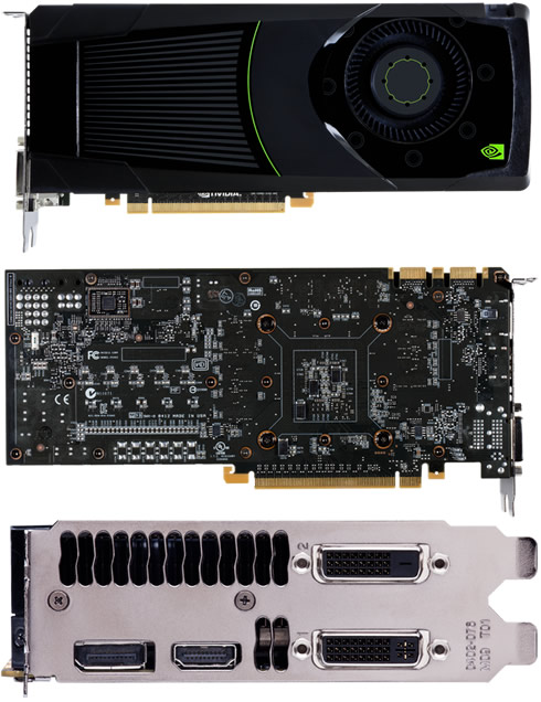
The design of the GeForce GTX 680 is not a very different than the GTX 580. The fan has been moved from the center of the card to the top of the card.
Looking at the top of the card, as always we see the SLI connectors : 2 SLI connectors, allowing for up to 3-way SLI.
The GTX 680 also features 2 DL-DVI ports, a full size HDMI port, and a full size DisplayPort.
GeForce GTX 680 is available today from e-tailers and system builders starting at $499. The first reviews of the card hint that the the GTX 680 is faster, cooler, and quieter than the rival AMD Radeon HD 7970, capturing the performance crown
GeForce 600M Reaches Ultrabooks
Nvidia today also introduced the NVIDIA GeForce 600M family of notebook GPUs.
The full GPU lineup includes:
- Enthusiast class – GeForce GTX 675M, GeForce GTX 670M, GeForce GTX 660M
- Performance class – GeForce GT 650M, GeForce GT 640M, GeForce GT 640M LE, GeForce GT 630M
- Mainstream class – GeForce GT 620M, GeForce 610M
Here are the specs:
| |
GeForce GTX 675M |
GeForce GTX 670M |
GeForce GTX 660M |
| GPU and Process |
40nm GF114 |
40nm GF114 |
28nm GK107 |
| CUDA Cores |
384 |
336 |
Up to 384 |
| GPU Clock |
620MHz |
598MHz |
835MHz |
| Shader Clock |
1240MHz |
1196MHz |
- |
| Memory Eff. Clock |
3GHz |
3GHz |
4GHz |
| Memory Bus |
256-bit |
192-bit |
128-bit |
| Memory Bandwidth |
96GB/s |
72GB/s |
64GB/s |
| Memory |
Up to 2GB GDDR5 |
Up to 3GB GDDR5 |
Up to 2GB GDDR5 |
| |
GeForce GT 650M |
GeForce GT 640M |
GeForce GT 640M LE |
| GPU and Process |
28nm GK107 |
28nm GK107 |
28nm GK107 |
40nm GF108 |
| CUDA Cores |
Up to 384 |
Up to 384 |
Up to 384 |
96 |
| GPU Clock |
850MHz |
625MHz |
500MHz |
762MHz |
| Shader Clock |
- |
- |
- |
1524MHz |
| Memory Bus |
128-bit |
128-bit |
128-bit |
128-bit |
| Memory Bandwidth |
Up to 64GB/s |
Up to 64GB/s |
Up to 28.8GB/s |
Up to 50.2GB/s |
| Memory |
Up to 2GB DDR3
or GDDR5 |
Up to 2GB DDR3
or GDDR5 |
Up to 2GB DDR3 |
Up to 2GB DDR3
or GDDR5 |
| |
GeForce GT 635M |
GeForce GT 630M |
GeForce GT 620M |
| GPU and Process |
40nm GF116 |
28nm/40nm GF108 |
28nm GF108 |
| CUDA Cores |
144 |
96 |
96 |
| GPU Clock |
675MHz |
800MHz |
625MHz |
| Shader Clock |
1350MHz |
1600MHz |
1250MHz |
| Memory Bus |
192-bit |
128-bit |
128-bit |
| Memory |
Up to 2GB GDDR5 |
Up to 2GB DDR3 |
Up to 1GB DDR3 |
Plus, NVIDIA Optimus technology with GeForce 600M Series GPUs help maximize battery life.
Many OEMs are already shipping GeForce 600M Series GPUs with Intel Sandy Bridge notebooks – for example, the Acer Aspire M3-581TG Ultrabook features a GeForce GT 640M.
Once Intel’s next-generation platform is fully rolled out, new notebooks with Nvidia's GPUs will be offered byAcer, Alienware, Asus, Dell, Gigabyte, HP, IBM, Lenovo, MSI, Samsung, Toshiba and newcomer Vizio.