|
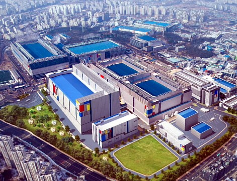
Samsung Electronics broke ground on a new EUV (extreme ultraviolet) line in Hwaseong, Korea, aiming to start production of 7nm chips in 2020.
Samsung expects the new facility to be completed within the second half of 2019 and start production ramp-up in 2020. The compay says that the initial investment in the new EUV line is projected to reach USD 6 billion by 2020, with additional investment to be determined depending on market circumstances.
Samsung has decided to utilize cutting-edge EUV technology starting with its 7-nanometer (nm) LPP (Low Power Plus) process. This new line will be set up with EUV lithography equipment to overcome nano-level technology limitations.
The company is also working with US chip giant Qualcomm on a 5G mobile chipset that will be made using the 7-nanometer process. Samsung developed a 8-nanometer process last October.
With this huge investment, Samsung appears to be preparing for a possible downturn in the memory chip market, as well as sharpening its competitive edge against the world's leading contract chipmaker, Taiwan Semiconductor Manufacturing Co.
Samsung is currently the world's fourth-place contract chipmaker, but aims to reach the No. 2 spot behind TSMC.
Apple (iPhones) is possibly the largest client of both Samsung and TSMC. The Taiwanese company has scored a string of wins in recent years, and appears to be in the lead for 2018 models of the smartphone as well, but some see Samsung staging a comeback with 2019 iPhone models.
About EUV
When producing semiconductor chips, silicon-based round disks, called "wafers" are coated with a light-sensitive substance and enter a system called a "scanner." Inside the scanner, a laser light source is cast onto the wafers to create patterns of circuitries, which later are used for forming billions of ultrafine, microscopically small structures, inside a semiconductor chip. This process, while described very concisely, is known as photolithography.
With EUV technology, a EUV system, or EUV scanner, will now be able to perform the photolithography step by utilizing a light source with an 'extreme ultraviolet' wavelength. In the world of chip manufacturing, realizing finer circuits is a must, as it enables integration of a greater number of components inside a chip and therefore building faster and more energy efficient chip.
The utilization of an EUV light source will allow for defining finer and denser patterns than previous methods because of its shorter wavelength, which is essential since light isn't able to directly define features smaller than its own wavelength. Upcoming EUV scanners will, specifically, utilize EUV radiation at a 13.5-nanometer wavelength, less than 1/10th of what current ArF excimer laser scanners are able to provide. |