|
|
Monday, March 19, 2012
|
Panasonic Develops 1-watt Chipset for Multi-gigabit
Millimeter Wave Wireless Communications
|
|
You are sending an email that contains the article
and a private message for your recipient(s). |
| Your Name: |
|
| Your e-mail: |
* Required! |
| Recipient (e-mail): |
* |
| Subject: |
* |
| Introductory Message: |
|
HTML/Text
(Photo: Yes/No) |
(At the moment, only Text is allowed...)
|
| |
|
| Message Text: |
Panasonic has managed to keep the power consumption of
its new multi-gigabit millimeter wave wireless
communication chipset down to 1 Watt, by employing a new
baseband processing architecture.
The new chipset will enable interactive communication
between various kinds of devices supporting the
specification developed by the WiGig Alliance. Panasonic
had previously developed fundamental CMOS circuit
technologies for 60 GHz transceiver and modem signal
processing circuits, but now an additional radio packet
processing block has been integrated as a key block of
the chipset.
 The chipset can be embedded into mobile
devices, such as smartphones, which require less than
1-Watt power consumption. This technology enables the
transfer a 30 minute-long compressed high-definition
video content to mobile devices within 10 seconds. It
also allows the streaming of latency-free high-definition
video (for example, instant high-definition display
updates in response to user controls on mobile devices)
directly from a mobile device onto a big screen TV with
real-time performance that surpasses any of the existing
technologies today. The chipset can be embedded into mobile
devices, such as smartphones, which require less than
1-Watt power consumption. This technology enables the
transfer a 30 minute-long compressed high-definition
video content to mobile devices within 10 seconds. It
also allows the streaming of latency-free high-definition
video (for example, instant high-definition display
updates in response to user controls on mobile devices)
directly from a mobile device onto a big screen TV with
real-time performance that surpasses any of the existing
technologies today.
With regard to high-speed wireless communication for
mobile devices, there is presently no practical solution
except for the wireless LAN technology that operates in
the 2.4 GHz and 5 GHz frequency bands. In the case of 60
GHz high-speed wireless communication devices, the band
range has been employed only by stationary devices, not
mobile devices, because wider frequency bands require
more power and wider chip surface. Panasonic has already
developed the basic 60 GHz band radio technologies for
mobile devices.
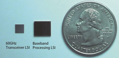
The newly developed chipset consists of a 60 GHz
transceiver LSI, and a baseband processing LSI with Media
Access Control (MAC) packet processing capability. Even
when operating at a high data rate of 2.5 Gigabits per
second, the chipset consumes less than 1-Watt of power.
The transceiver LSI size is reduced by more than 50%,
compared to the transceiver LSI Panasonic developed
earlier, while supporting 9 GHz bandwidth which is
allocated as unlicensed spectrum in Japan and Europe in
the 60 GHz frequency band.
The development of the chipset was part of the "research
and development project for expansion of radio spectrum
resources" of The Ministry of Internal Affairs and
Communications, Japan. |
|
|
|
|