GLOBALFOUNDRIES Unveils Its 14nm-XM FinFET Transistor Architecture
GLOBALFOUNDRIES today accelerated its roadmap with the launch of a new technology designed for the expanding mobile market.
The company's announced its 14nm-XM offering, which is expcted to offer performance and power benefits of three-dimensional "FinFET" transistors with less risk and a faster time-to-market.
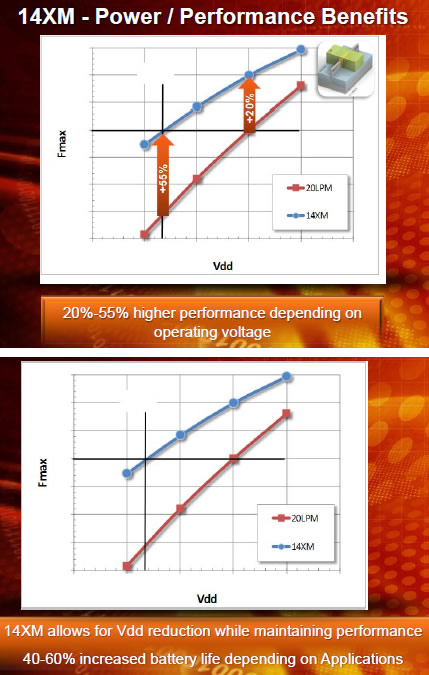
The XM stands for "eXtreme Mobility," and it is a non-planar architecture that is optimized for mobile system-on-chip (SoC) designs, providing a whole product solution from the transistor all the way up to the system level. When compared to today's 20nm planar technology, 14nm-XM is expected to deliver a 40-60% improvement in battery life and between 20-55% higher performance depending on operating voltage.
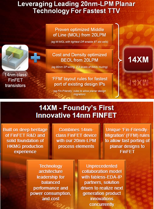
The 14nm-XM offering is based on a modular technology architecture that uses a 14nm FinFET device combined with elements of GLOBALFOUNDRIES' 20nm-LPM process, which is well on its way to production. GLOBALFOUNDRIES says that its 20nm offering has been well endorsed by the marketplace because it is the most comprehensive, cost-effective platform in the industry, delivering up to 40% performance improvement and twice the gate density of 28nm. Technology development is well underway and the company's Fab 8 in New York began running full-loop 20nm silicon in January.

The 14nm-XM technology leverages the Middle of Line (MOL) from 20nm-LPM with the tightest design rules to enable 8T standard cells, along with the cost and density advantages of the 20nm-LPM Back End of Line (BEOL). Technology development is already underway, with test silicon running through GLOBALFOUNDRIES' Fab 8 in Saratoga County, N.Y. Early process design kits (PDKs) are available now, with tape-outs expected in 2013.
"We have more than a decade of FinFET R&D to build on as we prepare to bring this technology to production," said Gregg Bartlett, Chief Technology Officer at GLOBALFOUNDRIES. "We are confident this foundation will enable us to lead the foundry volume ramp of FinFETs, just as we did with High-K Metal Gate (HKMG)."
The FinFET architecture takes the traditional two-dimensional transistor design and turns the conductive channel on its side, resulting in a three-dimensional "fin" structure surrounded by a gate that controls the flow of current. A key benefit of FinFET technology is its superior low-power attributes. The 3D transistor design intrinsically operates at a lower voltage with minimal current leakage, which translates into longer battery life for mobile applications or less power consumption for plugged-in applications such as networking chips in datacenters.
"Many people don't realize that FinFETs build upon the same fundamental mobile driving force as today's HKMG technology," said G. Dan Hutcheson, CEO and Chairman of VLSI Research. "While HKMG was a significant innovation in leakage reduction, FinFETs are a great leap forward in this value proposition that clear the way for many years of advancements. But to fully extract the value of FinFET technology, a company needs to be in volume production of HKMG. GLOBALFOUNDRIES has a head start in this area with almost two years of high-volume manufacturing experience with HKMG."
GLOBALFOUNDRIES claims that The 14nm-XM architecture "strikes the ideal balance between performance and power consumption, while minimizing both die size and cost." At the same time, the technology has been architected for optimum manufacturability and ease of design, with a view to allowing designers to re-use much of their IP from previous generations. Additionally, consideration is given to SoC-level concerns beyond the transistor architecture, such as overall system-level performance and specific mobile applications needs.
GLOBALFOUNDRIES recently announced a new multi-year agreement with ARM to jointly deliver optimized SoC solutions for ARM processor designs on FinFET process technologies. The companies have been collaborating for several years to jointly optimize ARM Cortex-A series processors, and this agreement extends the prior efforts by driving production IP platforms that will promote the migration to three-dimensional FinFET transistor technology.
"In the growing era of extreme mobility, FinFET technology will be a critical enabler to the next generation of smart mobile devices," said Dipesh Patel, deputy general manager of the Physical IP Division at ARM. "Through our early engagement and co-optimization with GLOBALFOUNDRIES, we will provide our mutual customers with a new level of system performance and an easier path to the benefits from FinFET technology. The result will be a platform which is well-suited for SoCs based on the next generation of ARM processors and GPUs for the mobile market."
The XM stands for "eXtreme Mobility," and it is a non-planar architecture that is optimized for mobile system-on-chip (SoC) designs, providing a whole product solution from the transistor all the way up to the system level. When compared to today's 20nm planar technology, 14nm-XM is expected to deliver a 40-60% improvement in battery life and between 20-55% higher performance depending on operating voltage.
The 14nm-XM offering is based on a modular technology architecture that uses a 14nm FinFET device combined with elements of GLOBALFOUNDRIES' 20nm-LPM process, which is well on its way to production. GLOBALFOUNDRIES says that its 20nm offering has been well endorsed by the marketplace because it is the most comprehensive, cost-effective platform in the industry, delivering up to 40% performance improvement and twice the gate density of 28nm. Technology development is well underway and the company's Fab 8 in New York began running full-loop 20nm silicon in January.
The 14nm-XM technology leverages the Middle of Line (MOL) from 20nm-LPM with the tightest design rules to enable 8T standard cells, along with the cost and density advantages of the 20nm-LPM Back End of Line (BEOL). Technology development is already underway, with test silicon running through GLOBALFOUNDRIES' Fab 8 in Saratoga County, N.Y. Early process design kits (PDKs) are available now, with tape-outs expected in 2013.
"We have more than a decade of FinFET R&D to build on as we prepare to bring this technology to production," said Gregg Bartlett, Chief Technology Officer at GLOBALFOUNDRIES. "We are confident this foundation will enable us to lead the foundry volume ramp of FinFETs, just as we did with High-K Metal Gate (HKMG)."
The FinFET architecture takes the traditional two-dimensional transistor design and turns the conductive channel on its side, resulting in a three-dimensional "fin" structure surrounded by a gate that controls the flow of current. A key benefit of FinFET technology is its superior low-power attributes. The 3D transistor design intrinsically operates at a lower voltage with minimal current leakage, which translates into longer battery life for mobile applications or less power consumption for plugged-in applications such as networking chips in datacenters.
"Many people don't realize that FinFETs build upon the same fundamental mobile driving force as today's HKMG technology," said G. Dan Hutcheson, CEO and Chairman of VLSI Research. "While HKMG was a significant innovation in leakage reduction, FinFETs are a great leap forward in this value proposition that clear the way for many years of advancements. But to fully extract the value of FinFET technology, a company needs to be in volume production of HKMG. GLOBALFOUNDRIES has a head start in this area with almost two years of high-volume manufacturing experience with HKMG."
GLOBALFOUNDRIES claims that The 14nm-XM architecture "strikes the ideal balance between performance and power consumption, while minimizing both die size and cost." At the same time, the technology has been architected for optimum manufacturability and ease of design, with a view to allowing designers to re-use much of their IP from previous generations. Additionally, consideration is given to SoC-level concerns beyond the transistor architecture, such as overall system-level performance and specific mobile applications needs.
GLOBALFOUNDRIES recently announced a new multi-year agreement with ARM to jointly deliver optimized SoC solutions for ARM processor designs on FinFET process technologies. The companies have been collaborating for several years to jointly optimize ARM Cortex-A series processors, and this agreement extends the prior efforts by driving production IP platforms that will promote the migration to three-dimensional FinFET transistor technology.
"In the growing era of extreme mobility, FinFET technology will be a critical enabler to the next generation of smart mobile devices," said Dipesh Patel, deputy general manager of the Physical IP Division at ARM. "Through our early engagement and co-optimization with GLOBALFOUNDRIES, we will provide our mutual customers with a new level of system performance and an easier path to the benefits from FinFET technology. The result will be a platform which is well-suited for SoCs based on the next generation of ARM processors and GPUs for the mobile market."