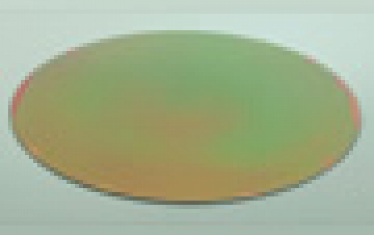
Samsung Tape Outs 32nm And 28nm Chips
Samsung Electronics said that it has already received 35 tape outs from its customers at 32nm and 28nm and many more are in the pipeline for tape out this year.
The company began its foundry business over six years ago with a focus on advanced technology nodes. With an aggressive process technology roadmap in place, the company set out to compete in an industry that was already seeing some consolidation.
Last year, 45nm became the majority volume runner in the company's 300mm S Line in Giheung. The ramp to production went very smoothly thanks to the company's vast experience with immersion lithography and technology. "The yield on this node has been excellent and we continue to drive improvements. Hand held devices powered by 45nm low power SoCs manufactured at Samsung for our customers are ubiquitous in the market today," said Ana Hunter, vice president of Samsung?s North American foundry services.
Last year, Samsung announced a new logic fab at our Austin, TX facility. Currently, that line is on schedule with 45nm low-power process qualified and Samsung's expectation is that this fab will be producing about 40,000 wafers per month by the end of 2011.
Samsung's 32nm LP High-k Metal Gate (HKMG) process node is also fully qualified with high yields and silicon proven design flows that are extendible to 28nm LP. Samsung?s ASIC Design Center also has a successful track record with design tape-outs at 32nm.
"As of today, we have received 35 tape outs from our customers at 32nm and 28nm and many more are in the pipeline for tape out this year. Customers are anxious to capitalize on the benefits of HKMG higher performance with lower power consumption," Ana Hunter added.
Samsung's executive believes that the company's foundry business "will be one of the few players to stretch down the process technology curve."