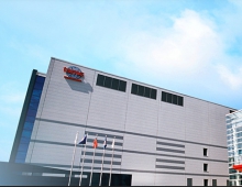
TSMC and MAPPER Reached Joint Development Milestone
Taiwan Semiconductor Manufacturing Company, the worlds largest dedicated semiconductor foundry and MAPPER Lithography today revealed that a pre-alpha MAPPER tool located on TSMCs Fab 12 GigaFab is repeatedly printing features previously unachievable using current immersion lithography technology.
Over the past several months TSMC has expanded its Maskless Lithography team and has been working with MAPPER engineers at Fab 12 to integrate electron beam direct write capabilities into manufacturing processes for development of future technology nodes.
MAPPER develops lithography machines for the chip industry. These machines utilize a new and technology with which the chips of the future can be made cost effectively. MAPPERs technology makes use of massively parallel electron beams, thereby providing the very high resolution of electron beam at extremely high throughput. Current lithography machines use photographic techniques to create minute electrical circuits smaller than 1/100th of a human hair on a silicon wafer. They use a mask that contains the blueprint of the chip and transfer this pattern on to a photosensitive layer (comparable to a photograph being exposed on film), however the photographic techniques used are very limited in the resolution they can provide and are no longer adequate for future generations of semiconductors.
"TSMC is always searching for the most cost effective manufacturing processes," says Dr. Shang-Yi Chiang, TSMC Senior Vice President of Research & Development. "The results coming from our project with MAPPER have met aggressive objectives and mark a significant achievement in our Multiple-E-Beam Direct Write program that covers all viable Multiple-E-Beam technologies. Based on these encouraging results, we are convinced that the Multiple E-Beam technology is one of the technologies to become the future lithography standard."
TSMC and MAPPER will present their latest results at the SPIE Advanced Lithography 2010 conference in San Jose, CA.