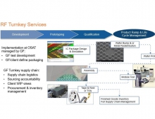
GLOBALFOUNDRIES To Highlight 32nm/28nm Technology at GSA Expo
On October 1 at the Global Semiconductor Alliance Emerging Opportunities Expo & Conference in Santa Clara, Calif., GLOBALFOUNDRIES will provide the latest details on its technology roadmap for the 32nm/28nm generations and its "Gate First" approach to building transistors based on High-K Metal Gate (HKMG) technology.
"With each new technology generation, semiconductor foundries are increasingly challenged with the economics to sustain R&D and the know-how to bring these technologies to market in high-volume," said Len Jelinek, director and chief analyst, iSuppli.
GLOBALFOUNDRIES expects to start volume production of 32nm-SHP (Super High Performance) technology at Fab 1 in the second half of 2010. This technology will employ silicon-on-insulator (SOI) substrates and utilize GLOBALFOUNDRIES? "Gate First" approach to HKMG, which maximizes power efficiency and transistor scaling while minimizing die size and design complexity when compared to the alternative "Gate Last" approach, according to the company. Yield progress continues with 24Mb SRAMs in double-digit natural yields on path to 50 per cent natural yields by year-end.
"When compared against the 45nm-SHP technology we?re currently running in Fab 1, we?re seeing performance improvements of up to 50 percent in the 32nm generation at the same leakage levels of the 45nm generation," said Jim Doran, senior vice president and general manager of Fab 1 at GLOBALFOUNDRIES. "When you combine this with our patented Automated Precision Manufacturing (APM) technology and exceptionally low defect densities, we believe we?ll be in the leading position among foundries to bring this technology to market in volume for our customers."
For the 28nm generation, which will be offered on bulk silicon substrates, the company will be accepting customer and third party IP designs in Q1 2010 on its shuttle service for low cost prototyping, with production planned in the second half of 2010. The 28nm technology offers the smallest SRAM cell size (0.120 ?m2) currently reported in the foundry industry, and an advantage in die size relative to 28nm "Gate Last" approaches. In addition, the GLOBALFOUNDRIES? "Gate First" approach to HKMG simplifies 28nm design implementation and IP re-use for customers using conventional poly/SiON-based technology at the 45/40nm and 32nm nodes due to similar process flows and design rules.
The 28nm node will be available in two variants: The 28nm-HP (High Performance) variant will be optimized for leading-edge applications in such areas as graphics, game consoles, storage, networking and media encoding. The 28nm-SLP (Super Low Power) variant is optimized for wireless mobile applications such as baseband, application processors, and other handheld functions that require long battery lifetime.
GLOBALFOUNDRIES? 32nm and 28nm technologies with the "Gate First" approach to HKMG were originally developed in partnership with IBM through the company?s participation in the IBM Technology Alliance. IBM and its research partners first introduced the "Gate First" HKMG innovation in 2007 as the basis for a long-sought improvement to the transistor to deal with power leakage that emerged at the 45nm node.