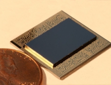
IBM Announces Industry's Densest, Fastest DRAM
IBM has successfully developed a prototype of the semiconductor industry's smallest and fastest on-chip dynamic memory device in next-generation, 32-nanometer, silicon-on-insulator (SOI) technology.
IBM's SOI technology can provide up to a 30 percent chip performance improvement and 40 percent power reduction, compared to standard bulk silicon technology. SOI protects the transistors on the chip with a "blanket" of insulation that reduces electrical leakage, saving power and allowing current to flow through the circuit more efficiently, improving performance.
IBM has fabricated a test chip with an embedded dynamic random access memory (eDRAM) technology that features the industry's smallest memory cell, and offers density, speed and capacity better than conventional on-chip static random access memory (SRAM) announced in 32nm and 22nm technology, and comparable to what would be expected of an SRAM produced in 15-nanometer technology - three technology generations ahead of chips in volume production today.
IBM's eDRAM cell is twice as dense as any announced 22nm embedded SRAM cell - including the world's smallest 22-nanometer memory cell announced by IBM in August 2008 - and up to four times as dense as any comparable 32nm embedded SRAM in the industry. Higher memory density can lead to chips that are smaller, more efficient and can process more data, improving system performance.
The IBM eDRAM in 32nm SOI technology is the fastest embedded memory announced to date, achieving latency and cycle times of less than 2 nanoseconds. In addition, the IBM eDRAM uses four times less standby power (power used by the chip as it sits idle) and has up to a thousand times lower soft-error rate (errors caused by electrical charges), offering better power savings and reliability compared to a similar SRAM.
Embedded memory is a key performance enabler for multi-core processors and other integrated circuits, and the new prototype has numerous implications for businesses and other organizations around the globe. For example, use of this technology in high-performance server, printer, storage and networking applications can result in improved system performance and energy savings. In mobile, consumer and game applications, it can result in a smaller system form-factor, lower-cost and energy savings.
IBM intends to bring the benefits of its 32-nanometer SOI technology to a wide range of application-specific integrated circuit (ASIC) and foundry clients and will use the technology in chips for its servers.
IBM already is engaged with early access foundry clients in 32nm technology and ARM is developing design libraries for the technology. An initial 32nm ARM library is available now and IBM has extended this collaboration to include 22nm SOI technology, enabling ARM to gain early access to this technology.
"We are making this 32nm offering available to clients who are ready to benefit from the significant performance and power advantages of this seventh generation of IBM SOI technology," said Gary Patton, vice president for IBM's Semiconductor Research and Development Center. "The industry-leading, dense embedded memory, and our design library agreement with ARM, underscore our ability to provide clients with a market edge and a clear progression path to 32nm and 22nm SOI technology nodes."
IBM engineers plan to describe the features of the 32nm and 22nm eDRAM at the International Electron Devices Meeting in December.
IBM was the first company to begin commercially shipping SOI technology, which has been used in applications from game consoles to servers.