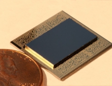
IBM and NEC to Jointly Develop Next-Generation Semiconductor Process Technology
IBM and NEC Electronics today announced they have entered into a multi-year joint development agreement under which they will develop next-generation semiconductor process technology.
Under the agreement, NEC Electronics will participate in a joint development project for the next-generation core CMOS process, at the 32-nm node, and in advanced fundamental research for leading-edge semiconductor technologies of the future.
NEC Electronics will be the eighth major semiconductor manufacturer represented in the IBM joint development alliances. Other members of the alliamce include Chartered Semiconductor Manufacturing, Freescale Semiconductor Infineon Technologies, Samsung Semiconductor, STMicroelectronics, Toshiba and ofcourse IBM.
"As the "scaling" of semiconductors to ever smaller feature sizes continues, the cost of conducting basic research and development and the associated capital investment continues to rise," said Gary Patton, vice president, IBM Semiconductor Research & Development Center. "Our unique collaborative model for semiconductor research and development helps to mitigate individual investment while allowing for increased design complexity, shortened time-to-market and quicker integration of next-generation process materials and technology nodes."
NEC Electronics co-develops the 45-nm and 32-nm CMOS process technology nodes with Toshiba and is now extending that scope of collaboration to include the 32-nm and finer nodes with IBM and its alliance partners. NEC Electronics intends to work with IBM and its research partners to develop a common process platform, and strengthen development and design ability in System-on-Chip (SoC).
"At the highest levels of technology, it is becoming increasingly difficult for semiconductor companies to differentiate their products on the core CMOS process technologies alone. A better course is to share the development costs of a common process platform with leading semiconductor manufacturers from around the world." said Toshio Nakajima, President and CEO, NEC Electronics. " The new agreement with IBM means that NEC Electronics will develop a common semiconductor process with industry leaders, allowing us to focus on being first to market in areas of eDRAM products and SoC solutions that provide our customers with the added value, such as high reliability and low power consumption."
The work will be conducted at IBM's 300 millimeter (mm) semiconductor fabrication facility in East Fishkill, N.Y. and at the College of Nanoscale Science and Engineering (CNSE) of the University at Albany, State University of New York. CNSE's Albany NanoTech is the world's most advanced university-based nanoelectronics research complex.
Earlier this year, IBM and its partners unveiled significant performance and power advantages over industry standards by using a breakthrough material known as "high-k/metal gate" (HKMG) on silicon manufactured at IBM's 300 millimeter semiconductor fabrication facility in East Fishkill, N.Y. By implementing "high-k/metal gate" technology into its 32nm technology node, the alliance has assessed performance improvements in circuits of up to 35 percent over 45nm technology at the same operating voltage. The 32-nm power reduction over 45nm can be as much as 30 to 50 percent depending on the operating voltage.