IBM and partners Build World's Smallest SRAM Memory Cell
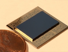
IBM and its joint development partners - AMD, Freescale, STMicroelectronics, Toshiba and the College of Nanoscale Science and Engineering (CNSE) - today announced the first working static RAM (SRAM) for the 22 nm technology node, the world's first reported working cell built at its 300mm research facility in Albany, NY.
SRAM chips are precursors to more complex devices such as microprocessors.
The SRAM cell utilizes a conventional six-transistor design and has an area of 0.1um2, breaking the previous SRAM scaling barriers.
Researchers achieved this breakthrough at CNSE of the University at Albany, State University of New York. CNSE's Albany NanoTech is the world's most advanced university based nanoelectronics research complex. IBM and its partners do much of their leading-edge semiconductor research at CNSE.
A nanometer is one one-billionth of a meter or about 80,000 times smaller than the width of a human hair.
"We are working at the ultimate edge of what is possible -- progressing toward advanced, next-generation semiconductor technologies," said Dr. T.C. Chen, vice president of Science and Technology, IBM Research. "This new development is a critical achievement in the pursuit to continually drive miniaturization in microelectronics."
22 nm is two generations away in chip manufacturing. The next generation is 32 nm -- where IBM and its partners are in development with their leading 32 nm high-K metal gate technology that no other company or consortium can match.
Traditionally, an SRAM chip is made more dense by shrinking its basic building block, often referred to as a cell. IBM-alliance researchers optimized the SRAM cell design and circuit layout to improve stability and developed several novel fabrication processes in order to make the new SRAM cell possible. The researchers utilized high-NA immersion lithography to print the aggressive pattern dimensions and densities and fabricated the parts in its a state-of-the-art 300mm semiconductor research environment.
SRAM cell size is a key technology metric in the semiconductor industry, and this work demonstrates IBM and its partners' continued leadership in cutting-edge process technology.
Key enablers of the SRAM cell include band edge high-K metal gate stacks, transistors with less than 25 nm gate lengths, thin spacers, novel co-implants, advanced activation techniques, extremely thin silicide, and damascene copper contacts.
Additional details of this achievement will be presented at the IEEE International Electron Devices (IEDM) annual technical meeting to be held in San Francisco, CA, December 15-17, 2008.