Samsung Unveils New Fusion Memory Solution - OneDRAM
Samsung today announced that it has developed a prototype fusion
memory chip that can significantly increase the data processing
speed between processors in mobile applications.
Samsung's new fusion solution OneDRAM is expected to be specified
in the design of handsets, game consoles and in other digital
applications, especially those that use 3-dimensional graphics.
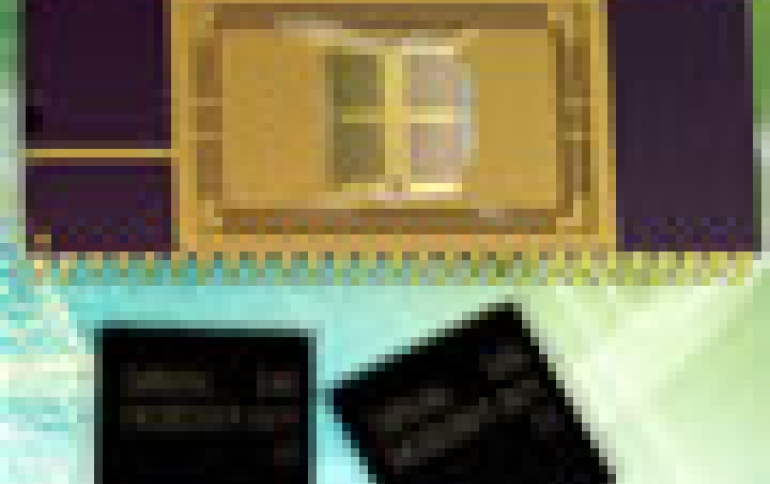
The 133MHz 512Mb device incorporates a dual-port approach to increase the time that it takes to transfer data between processors. Data managed by the processors is housed in a shared bank where the space for storing data can be adjusted accordingly. This meets the JEDEC low power double-data-rate (LPDDR) memory standard.
Due to rapidly increasing demand for multimedia features in mobile applications, designers have been specifying the use of two separate processors ? a communication processor and a media processor. The new OneDRAM will channel data between the processors through a single chip eliminating the need to also specify DRAM and SRAM chips for buffer memory.
"Along with the faster data processing speeds between the processors, the OneDRAM reduces power consumption by 30 percent, lessens the number of chips needed and minimizes area coverage by 50 percent, resulting in a five-fold increase in the speed of cell phone and gaming console operations, longer battery life and slimmer handset designs," said Samsung in a statement.
A single OneDRAM can replace, at least, two mobile memories in smart phones and other multimedia-rich handsets.
Samsung expects its OneDRAM to be introduced in handsets by the second half of 2007.
NAND flash memory
In related news, Dr. Chang-Gyu Hwang, president and CEO of Samsung Electronics' Semiconductor Business, presented a paper that focuses on the development of NAND flash memory based on charge trap flash (CTF) technology, at the plenary session of the 2006 International Electron Devices Meeting (IEDM).
NAND flash memory based on charge trap flash (CTF) technology is expected to be the basis for producing 32-gigabit NAND memory in the near future using 40-nanometer process technology, Hwang said.