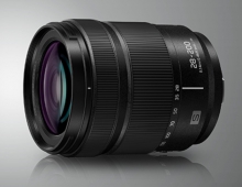
Panasonic Starts Production of 65 nm LSIs at New 300 mm Wafer Fab
Panasonic today announced that the company will start shipping mass-produced system LSIs using a 65-nanometer process technology at the end of October from its Uozu Plant in Toyama Prefecture, central Japan.
The shipment schedule has been moved up two months earlier than planned in order to fulfill the increasing world demand for advanced system LSIs.
"The new fab uses the large 300 mm-diameter wafer manufacturing technology. By implementing the 65 nm process ahead of the original schedule, we have stepped up the pace in achieving higher productivity and fine patterning technologies that are required for sophisticated consumer electronic devices. We are focusing on five key product areas including DVDs, digital TVs, mobile communications equipment, SD Memory Cards and SD applied products as well as CCD (charge coupled device) image sensors."
The new fab starts with a monthly output capacity of 6,500 wafers. The 65 nm process technology uses nickel silicide, resolution enhancement technology and copper interconnect to ensure stable production. The technology allows low-power consumption and high-speed processing, as well as high transistor density at the same time. The first 65 nm LSI is to be used for DVD-related products, making them more compact with advanced features.
The Japanese giant has invested approximately 130 billion yen (US $1,125,833,549) on the new 77,000 square meters plant, and plans to release 6,500 wafers per month (300-mm wafer/65-nm process technology).