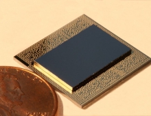
IBM shrinks SRAM cells, triples transistor performance
IBM said that it has built the world's smallest SRAM cell
and demonstrated for the first time transistors built with strained germanium that can
deliver three times the performance of today's transistors.
Providing an outlook three SRAM generations ahead, IBM said that its memory cell is about
ten times smaller than those of common SRAM cells available on the market today, which
measure around 1 ΅m2. IBM's said that the cell also is about half the size of the
smallest experimental cell reported to date and cut fit 50,000 of those cells on circular
end of a human hair. The company said that it will provide further details about the
technology at the upcoming International Electron Devices Meeting in December.
IBM is not alone in the field of shrinking SRAM cells to be able to increase SRAM capacity especially in processors. Texas Instruments announced earlier this year, that it produced a 0.49 ΅m2 SRAM cell in 65 nm process technology with about 930,000 logic gates per mm2.
IBM on Monday also said that it has demonstrated a technique that triples the performance of a standard transistor used in semiconductors by creating a layer of germanium in the portion of the transistor through which electrical current flows, called the "channel." Germanium has long been known to have better conductivity than silicon, and the strain in the germanium layer created by IBM's process leads to further performance gains, the company said.
The introduction of a new material like germanium in the critical areas of the integrated circuits provides an alternative means of improving chip performance from the traditional method of simply shrinking circuitry, according to IBM. The company hopes that this new technique will help to achieve performance improvements in chips with circuit sizes of 32 nm and smaller.